CORE-V MCU DevKit Hardware Description
Feature List
The CORE-V MCU DevKit includes these features:
CORE-V MCU
CV32E40P processor core
Quicklogic ArticPro 2 eFPGA
4 MB flash memory
Ashling Opella-LD onboard JTAG debug module
USB-C for terminal and onboard debug access
JTAG connector for external debug access
Espressif AWS IoT ExpressLink Module for AWS IoT cloud interconnect
mikroBUS onboard socket, allowing access to a vast range of mikroBUS modules
Himax HM01B0 Ultralow Power CMOS Image Sensor
I2C temperature sensor
Several LEDs
Reset button and general purpose button
Dimensions 75 mm x 100 mm
Power supply via USB-C or barrel connector (5V - 18V in)
Architecture diagram
The figure below provides a block-diagram view of the DevKit.
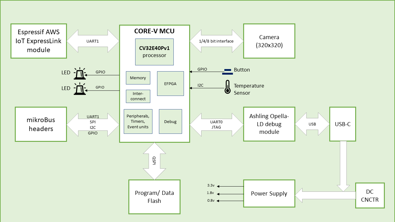
DevKit Block Diagram
Board layout
The DevKit board measures 75 mm x 100 mm.
The figure below provides a top elevation visualization of the DevKit
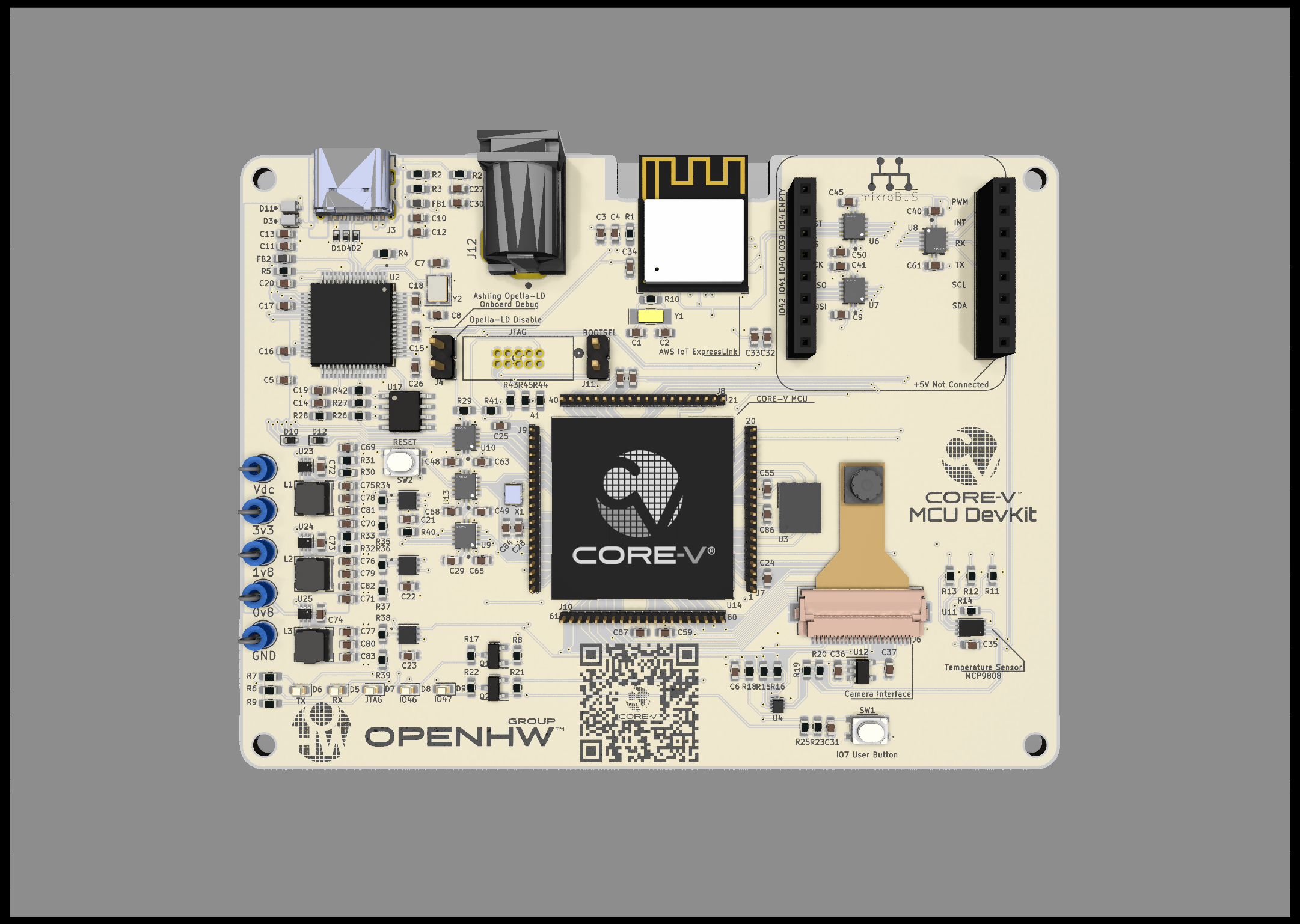
DevKit Visualization (Top view)
The figure below provides a angle (isometric) elevation visualization of the DevKit
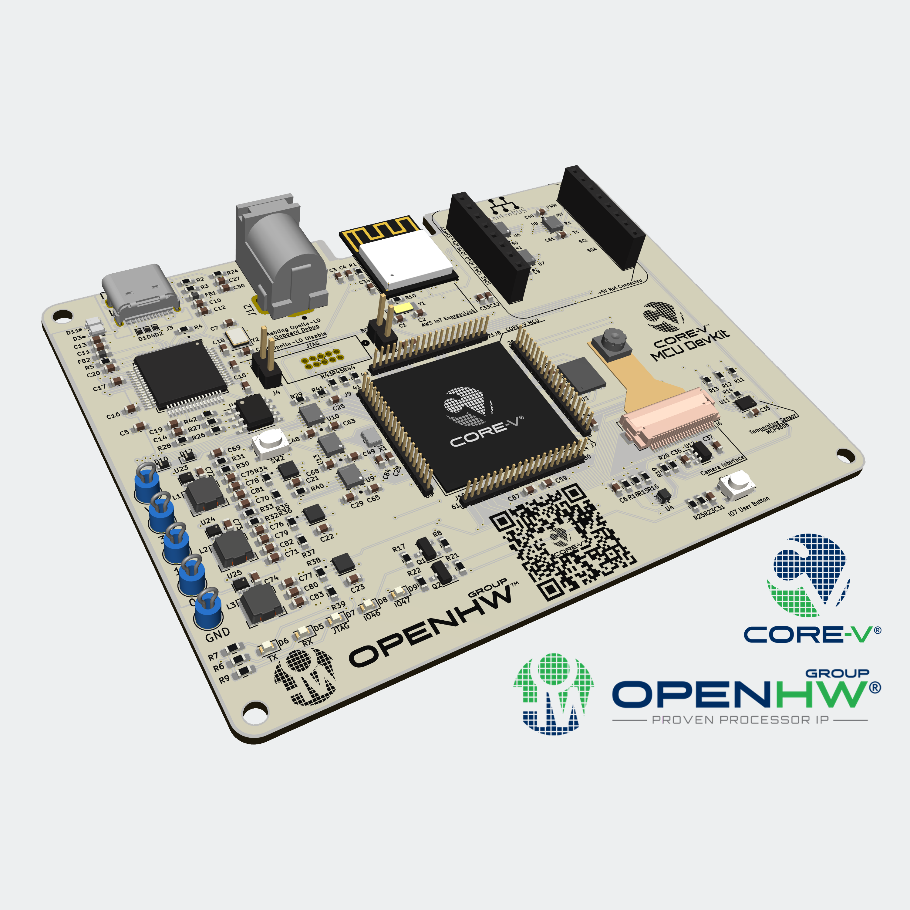
DevKit Visualization (Angle view)
Component Description
We review below the DevKits’s main components and provide links for further information.
CORE-V MCU
At the heart of the DevKit is the CORE-V MCU, an ASIC developed by the OpenHW community and fabricated in Global Foundry’s 22FDX process The CORE-V MCU provides an evaluation and development platform for OpenHW’s fully-verified CV32E40PV1.0 embedded-class processor core. The CORE-V-MCU integrates the processor core with a set of on-chip peripherals, memory, and Quicklogic’s embedded FPGA (eFPGA) technology. The CORE-V MCU logic, with the exception of the eFPGA, is available on Github in open-source RTL under the permissive Solderpad 2.1 license.
CV32E40PV1.0 Processor Core
The CV32E40P processor core is the first core released by OpenHW Group on Github in open-source RTL. It is a 4-stage, in-order 32-bit RISC-V processor core. The CV32E40P, developed through the collaborative efforts of the OpenHW community, is completely open-source and released under the permissive Solderpad 2.1 license. The ISA instruction set of of CV32E40P as instantiated within the CORE-V-MCU is shown here.
On-Chip Memory
The CORE-V MCU includes 512K-byte of on-chip SRAM. The memory is organized as two 32K-byte banks of non-interleaved SRAM, typically used for program store, plus four 112K-byte banks of interleaved SRAM, typically used for data store. The interleaved memory architecture provides high speed access to memories for both the processor core and I/O peripherals.
On-Chip Peripherals
The CORE-V MCU includes the following peripherals: 2 UARTs 2 QSPI masters 2 I2C masters 1 SDIO 1 CI (Camera) 1 GPIO unit with 32 I/O 1 I2C slave 1 Advanced Timer (PWM) with 4 channels JTAG
Embedded FPGA (eFPGA)
The embedded FPGA (eFPGA) subsystem integrated within the CORE-V MCU is based on Quicklogic’s ArcticPro 2 architecture. This is a silicon-verified, production-proven eFPGA for MCU/SoC/custom ASIC applications. The eFPGA IP enables the flexibility to easily program custom functions, hardware accelerators and security algorithms after an SoC has been manufactured. Programming the eFPGA within CORE-V MCU will be supported by Open Source tools to create the bitstream. Example designs will be provided.
CORE-V MCU DevKit Expresslink Module
The CORE-V MCU DevKit includes Espressif’s AWS IoT ExpressLink module , which provides WiFi and out-of-the-box, seamless connectivity to the AWS IoT ExpressLink cloud service. This allows DevKit-based IoT applications, such as the OpenHW-developed temperature sensing demonstration to interconnect with AWS IoT cloud services.
CORE-V MCU DevKit MikroBus Header
The CORE-V MCU DevKit includes a mikroBUS™ socket, comprising a pair of 1×8 female headers that support interconnection to a wide range of display, sensor, actuator and other modules.
CORE-V MCU DevKit Debug Interface
The CORE-V MCU DevKit supports on-chip debugging of the CORE-V MCU via a JTAG interface and board connector. Additionally, the debug signals are converted to USB via the Ashling Opella-LD debug probe and brought out on USB-C.
CORE-V MCU DevKit Flash Memory
The CORE-V MCU DevKit provides a 4 MB flash memory used to store program code and other data. In the case of program code, a CORE-V MCU ROM-based bootloader loads the flash memory into the CORE-V MCU internal 512 KB SRAM.
CORE-V MCU DevKit Camera
The CORE-V MCU DevKit supports a Himax camera (Ultra Low Power CMOS Image Sensor) connected to the CORE-V MCU via Camera Serial Interface . The camera is mounted on a flex cable that allows the user to orient the camera in a variety of directions.
CORE-V MCU DevKit Power Supply
The CORE-V MCU DevKit includes a switching power supply which can accept 5V from the USB-C, or 5V - 18 V from the 2.1 mm barrel connector.
CORE-V MCU Pinout Table:
Pin # |
MUX 0 |
MUX 1 |
MUX 2 |
MUX 3 |
Devkit Usage |
|---|---|---|---|---|---|
IO0 |
TCK |
JTAG Function |
|||
IO1 |
TDI |
JTAG Function |
|||
IO2 |
TDO |
JTAG Function |
|||
IO3 |
TMS |
JTAG Function |
|||
IO4 |
TRST |
JTAG Function |
|||
IO5 |
10MHz Clock |
System Clock |
|||
IO6 |
Reset |
Reset |
|||
IO7 |
UART0 RX |
APB IO 0 |
FPGA IO 0 |
Console Serial RX |
|
IO8 |
UART0 TX |
APB IO 1 |
FPGA IO 1 |
Console Serial TX |
|
IO9 |
UART1 TX |
APB IO 2 |
FPGA IO 2 |
MikroBus Serial TX |
|
IO10 |
UART1 RX |
APB IO 3 |
FPGA IO 3 |
MikroBus Serial RX |
|
IO11 |
UART1 TX |
APB IO 4 |
FPGA IO 4 |
ExpressLink Serial TX |
|
IO12 |
UART1 RX |
APB IO 5 |
FPGA IO 5 |
ExpressLink Serial RX |
|
IO13 |
QSPI0 CS |
APB IO 34 |
APB IO 6 |
FPGA IO 6 |
Program Flash Chip Select |
IO14 |
QSPI0 Data 0 |
APB IO 35 |
APB IO 7 |
FPGA IO 7 |
Program Flash Data 0 |
IO15 |
QSPI0 Data 1 |
APB IO 37 |
APB IO 8 |
FPGA IO 8 |
Program Flash Data 1 |
IO16 |
QSPI0 CLK |
APB IO 9 |
FPGA IO 9 |
Program Flash Clock |
|
IO17 |
APB IO 1 |
APB IO 40 |
APB IO 10 |
FPGA IO 10 |
User Button |
IO18 |
APB IO 2 |
APB IO 41 |
APB IO 11 |
FPGA IO 11 |
MikroBus Reset Signal |
IO19 |
QSPI0 Data 2 |
APB IO 42 |
APB IO 12 |
FPGA IO 12 |
Program Flash Data 2 |
IO20 |
QSPI0 Data 3 |
APB IO 43 |
APB IO 13 |
FPGA IO 13 |
Program Flash Data 3 |
IO21 |
CAM0 VSYNC |
APB IO 36 |
APB IO 14 |
FPGA IO 14 |
Camera Vsync |
IO22 |
CAM0 HSYNC |
APB IO 39 |
APB IO 15 |
FPGA IO 15 |
Camera Hsync |
IO23 |
I2C0 SCL |
APB IO 16 |
FPGA IO 16 |
ExpressLink Wake |
|
IO24 |
I2C0 SDA |
APB IO 17 |
FPGA IO 17 |
ExpressLink Event |
|
IO25 |
CAM0 CLK |
APB IO 33 |
APB IO 18 |
FPGA IO 18 |
Camera P-Clock |
IO26 |
APB IO 32 |
QSPI0 CS1 |
APB IO 19 |
FPGA IO 19 |
Camera M-Clock |
IO27 |
APB IO 48 |
QSPI0 CS2 |
APB IO 20 |
FPGA IO 20 |
GPIO LED |
IO28 |
APB IO 49 |
QSPI0 CS3 |
APB IO 21 |
FPGA IO 21 |
FPGA LED (or GPIO LED) |
IO29 |
CAM0 Data 0 |
APB IO 22 |
FPGA IO 22 |
Camera Data 0 |
|
IO30 |
CAM0 Data 1 |
APB IO 23 |
FPGA IO 23 |
Camera Data 1 |
|
IO31 |
CAM0 Data 2 |
APB IO 24 |
FPGA IO 24 |
Camera Data 2 |
|
IO32 |
CAM0 Data 3 |
APB IO 25 |
FPGA IO 25 |
Camera Data 3 |
|
IO33 |
CAM0 Data 4 |
APB IO 26 |
FPGA IO 26 |
Camera Data 4 |
|
IO34 |
CAM0 Data 5 |
APB IO 27 |
FPGA IO 27 |
Camera Data 5 |
|
IO35 |
CAM0 Data 6 |
APB IO 28 |
FPGA IO 28 |
Camera Data 6 |
|
IO36 |
CAM0 Data 7 |
APB IO 29 |
FPGA IO 29 |
Camera Data 7 |
|
IO37 |
SDIO0 Data 3 |
APB IO 30 |
FPGA IO 30 |
MikroBus Interrupt |
|
IO38 |
SDIO0 Cmd |
APB IO 31 |
FPGA IO 31 |
MikroBus CS |
|
IO39 |
SDIO0 Data 0 |
APB IO 32 |
FPGA IO 32 |
MikroBus MOSI |
|
IO40 |
SDIO0 CLK |
APB IO 43 |
FPGA IO 33 |
MikroBus CLK |
|
IO41 |
SDIO0 Data 1 |
APB IO 44 |
FPGA IO 34 |
MikroBus MISO |
|
IO42 |
SDIO0 Data 1 |
APB I0 45 |
FPGA IO 35 |
MikroBus PWM |
|
IO43 |
APB IO 50 |
APB IO 0 |
APB IO 46 |
FPGA IO 36 |
ExpressLink Reset |
IO44 |
BOOTSEL |
||||
IO45 |
TEST MODE |
||||
IO46 |
I2C1 SCL |
FPGA IO 37 |
I2C0 SCL |
||
IO47 |
I2C1 SDA |
FPGA IO 38 |
I2C0 SDA |
Schematic
The figure below provides a schematic for the DevKit.
DevKit Schematics
Getting started with the DevKit
s Meant to go here: configuration of any jumpers and switches and connection of the power supplies etc.