Introduction
CV32E40P is a 4-stage in-order 32-bit RISC-V processor core. The ISA of CV32E40P has been extended to support multiple additional instructions including hardware loops, post-increment load and store instructions and additional ALU instructions that are not part of the standard RISC-V ISA. Figure 1 shows a block diagram of the core.
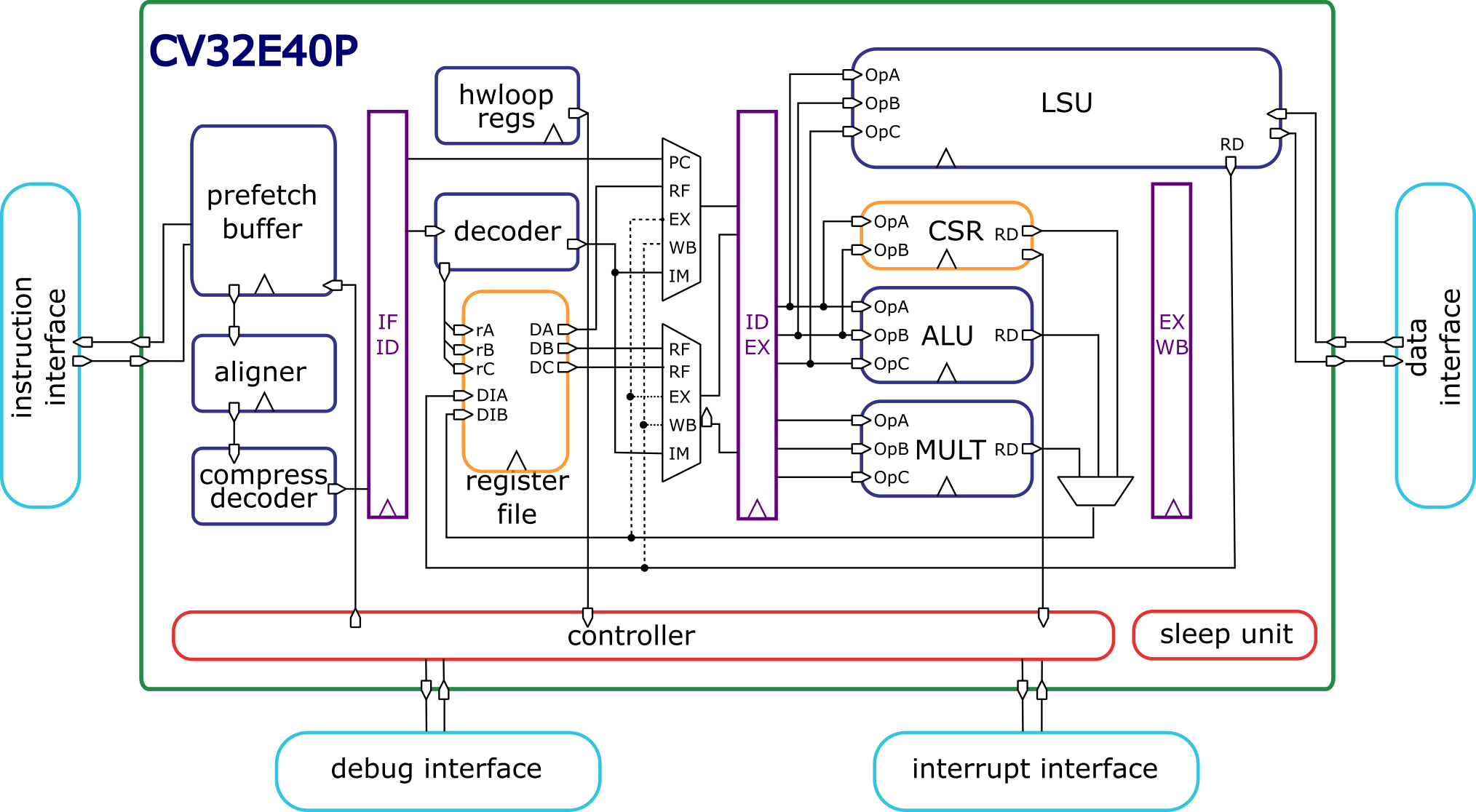
Figure 1 Block Diagram of CV32E40P RISC-V Core
License
Copyright 2020 OpenHW Group.
Copyright 2018 ETH Zurich and University of Bologna.
Copyright and related rights are licensed under the Solderpad Hardware License, Version 0.51 (the “License”); you may not use this file except in compliance with the License. You may obtain a copy of the License at http://solderpad.org/licenses/SHL-0.51. Unless required by applicable law or agreed to in writing, software, hardware and materials distributed under this License is distributed on an “AS IS” BASIS, WITHOUT WARRANTIES OR CONDITIONS OF ANY KIND, either express or implied. See the License for the specific language governing permissions and limitations under the License.
Standards Compliance
CV32E40P is a standards-compliant 32-bit RISC-V processor. It follows these specifications:
RISC-V Instruction Set Manual, Volume II: Privileged Architecture, document version 20190608-Base-Ratified (June 8, 2019). CV32E40P implements the Machine ISA version 1.11.
Many features in the RISC-V specification are optional, and CV32E40P can be parametrized to enable or disable some of them.
CV32E40P supports the following base instruction set.
The RV32I Base Integer Instruction Set, version 2.1
In addition, the following standard instruction set extensions are available.
Standard Extension |
Version |
Configurability |
|---|---|---|
C: Standard Extension for Compressed Instructions |
2.0 |
always enabled |
M: Standard Extension for Integer Multiplication and Division |
2.0 |
always enabled |
Zicount: Performance Counters |
2.0 |
always enabled |
Zicsr: Control and Status Register Instructions |
2.0 |
always enabled |
Zifencei: Instruction-Fetch Fence |
2.0 |
always enabled |
F: Single-Precision Floating-Point |
2.2 |
optionally enabled based on |
The following custom instruction set extensions are available.
Custom Extension |
Version |
Configurability |
|---|---|---|
Xcorev: CORE-V ISA Extensions (excluding cv.elw) |
1.0 |
optionally enabled based on |
Xpulpcluster: PULP Cluster Extension |
1.0 |
optionally enabled based on |
Xpulpzfinx: PULP Share Integer (X) Registers with Floating Point (F) Register Extension |
1.0 |
optionally enabled based on |
Most content of the RISC-V privileged specification is optional. CV32E40P currently supports the following features according to the RISC-V Privileged Specification, version 1.11.
M-Mode
All CSRs listed in Control and Status Registers
Hardware Performance Counters as described in Performance Counters based on
NUM_MHPMCOUNTERSparameterTrap handling supporting direct mode or vectored mode as described at Exceptions and Interrupts
Synthesis guidelines
The CV32E40P core is fully synthesizable. It has been designed mainly for ASIC designs, but FPGA synthesis is supported as well.
All the files in the rtl and rtl/include folders are synthesizable.
The user should first decide whether to use the flip-flop or latch-based register-file ( see Register File).
Secondly, the user must provide a clock-gating module that instantiates the clock-gating cells of the target technology. This file must have the same interface and module name of the one provided for simulation-only purposes
at bhv/cv32e40p_sim_clock_gate.sv (see Clock Gating Cell).
The rtl/cv32e40p_pmp.sv should not be included in the synthesis scripts as it is not supported.
This file is kept in the repository as a starting-point for users that want to implement their own.
The constraints/cv32e40p_core.sdc file provides an example of synthesis constraints.
ASIC Synthesis
ASIC synthesis is supported for CV32E40P. The whole design is completely synchronous and uses positive-edge triggered flip-flops, except for the register file, which can be implemented either with latches or with flip-flops. See Register File for more details. The core occupies an area of about 50 kGE when the latch based register file is used. With the FPU, the area increases to about 90 kGE (30 kGE FPU, 10 kGE additional register file). A technology specific implementation of a clock gating cell as described in Clock Gating Cell needs to be provided.
FPGA Synthesis
FPGA synthesis is supported for CV32E40P when the flip-flop based register file is used. Since latches are not well supported on FPGAs, it is crucial to select the flip-flop based register file. The user needs to provide a technology specific implementation of a clock gating cell as described in Clock Gating Cell.
Verification
The verification environment (testbenches, testcases, etc.) for the CV32E40P core can be found at core-v-verif. It is recommended that you start by reviewing the CORE-V Verification Strategy.
In early 2021 the CV32E40P achieved Functional RTL Freeze, meaning that is has been fully verified as per its Verification Plan. The top-level README in core-v-verif has a link to the final functional, code and test coverage reports.
The unofficial start date for the CV32E40P verification effort is 2020-02-27, which is the date the core-v-verif environment “went live”. Between then and RTL Freeze, a total of 47 RTL issues and 38 User Manual issues were identified and resolved 1. A breakdown of the RTL issues is as follows:
“Found By” |
Count |
Note |
|---|---|---|
Simulation |
18 |
See classification below |
Inspection |
13 |
Human review of the RTL |
Formal Verification |
13 |
This includes both Designer and Verifier use of FV |
Lint |
2 |
|
Unknown |
1 |
A classification of the simulation issues by method used to identify them is informative:
Simulation Method |
Count |
Note |
|---|---|---|
Directed, self-checking test |
10 |
Many test supplied by Design team and a couple from the Open Source Community at large |
Step & Compare |
6 |
Issues directly attributed to S&C against ISS |
Constrained-Random |
2 |
Test generated by corev-dv (extension of riscv-dv) |
A classification of the issues themselves:
Issue Type |
Count |
Note |
|---|---|---|
RTL Functional |
40 |
A bug! |
RTL coding style |
4 |
Linter issues, removing TODOs, removing `ifdefs, etc. |
Non-RTL functional |
1 |
Issue related to behavioral tracer (not part of the core) |
Unreproducible |
1 |
|
Invalid |
1 |
Additional details are available as part of the CV32E40P v1.0.0 Report.
Contents
Getting Started with CV32E40P discusses the requirements and initial steps to start using CV32E40P.
Core Integration provides the instantiation template and gives descriptions of the design parameters as well as the input and output ports.
CV32E40P Pipeline described the overal pipeline structure.
The instruction and data interfaces of CV32E40P are explained in Instruction Fetch and Load-Store-Unit (LSU), respectively.
The two register-file flavors are described in Register File.
Auxiliary Processing Unit (APU) describes the Auxiliary Processing Unit (APU).
Floating Point Unit (FPU) describes the Floating Point Unit (FPU).
Sleep Unit describes the Sleep unit including the PULP Cluster extension.
CORE-V Hardware Loop Extensions describes the PULP Hardware Loop extension.
The control and status registers are explained in Control and Status Registers.
Performance Counters gives an overview of the performance monitors and event counters available in CV32E40P.
Exceptions and Interrupts deals with the infrastructure for handling exceptions and interrupts.
Debug & Trigger gives a brief overview on the debug infrastructure.
Tracer gives a brief overview of the tracer module.
CORE-V Instruction Set Extensions describes the custom instruction set extensions.
Glossary provides definitions of used terminology.
History
CV32E40P started its life as a fork of the OR10N CPU core that is based on the OpenRISC ISA. Then, under the name of RI5CY, it became a RISC-V core (2016), and it has been maintained by the PULP platform <https://pulp-platform.org> team until February 2020, when it has been contributed to OpenHW Group https://www.openhwgroup.org>.
References
Contributors
Michael Gautschi (*gautschi@iis.ee.ethz.ch*)
Pasquale Davide Schiavone (*pschiavo@iis.ee.ethz.ch*)
Arjan Bink (*arjan.bink@silabs.com*)
Paul Zavalney (*paul.zavalney@silabs.com*)
- 1
It is a testament on the quality of the work done by the PULP platform team that it took a team of professonal verification engineers more than 9 months to find all these issues.