Pipeline Details
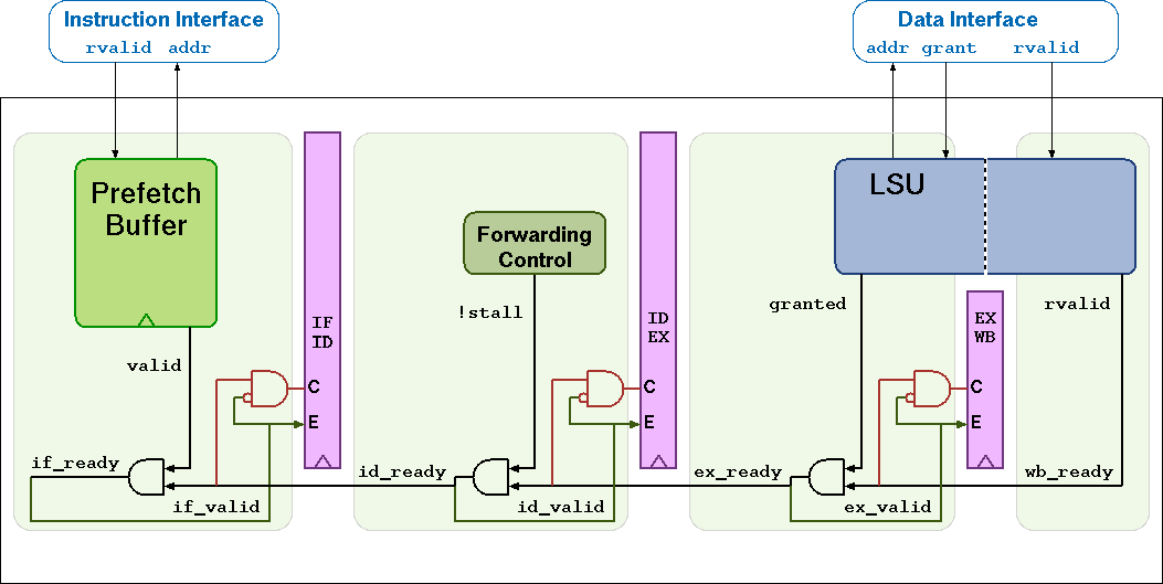
Figure 5 CV32E40P Pipeline
CV32E40P has a 4-stage in-order completion pipeline, the 4 stages are:
- Instruction Fetch (IF)
Fetches instructions from memory via an aligning prefetch buffer, capable of fetching 1 instruction per cycle if the instruction side memory system allows. This prefetch buffer is able to store 2 32-b data. The IF stage also pre-decodes RVC instructions into RV32I base instructions. See Instruction Fetch for details.
- Instruction Decode (ID)
Decodes fetched instruction and performs required register file reads. Jumps are taken from the ID stage.
- Execute (EX)
Executes the instructions. The EX stage contains the ALU, Multiplier and Divider. Branches (with their condition met) are taken from the EX stage. Multi-cycle instructions will stall this stage until they are complete. The ALU, Multiplier and Divider instructions write back their result to the register file from the EX stage. The address generation part of the load-store-unit (LSU) is contained in EX as well.
The FPU writes back its result at EX stage as well through this ALU/Mult/Div register file write port when FPU_*_LAT is either 0 cycle or greater than 1 cycle. When FPU_*_LAT > 1, FPU write-back has the highest priority so it will stall EX stage if there is a conflict. There are few exceptions to this FPU priority over ALU/Mult/Div.
They are:
There is a multi-cycle MULH in EX.
There is a Misaligned LOAD/STORE in EX.
There is a Post-Increment LOAD/STORE in EX.
In those 3 exceptions, EX will not be stalled, FPU result (and flags) are memorized and will be written back in the register file (and FPU CSR) as soon as there is no conflict anymore.
- Writeback (WB)
Writes the result of Load instructions back to the register file.
The FPU writes back its result from WB stage as well when FPU_*_LAT is 1 cycle. It is reusing register file LSU write port but LSU has the highest priority over FPU if there is a conflict.
Hazards
There is a forwarding path betwen ALU, Multiplier and Divider result in EX stage and ID stage flip-flops to avoid the need of a write-through register file. This allows to have 0-cycle penalty between those instructions and immediately following one when using result. This is the same with 0-cycle latency FPU instructions.
But the CV32E40P experiences a 1-cycle penalty on the following hazards:
Load data hazard in case the instruction immediately following a load uses the result of that load
Jump register (jalr) data hazard in case that a jalr depends on the result of an immediately preceding instruction
FPU data hazard when FPU_*_LAT = 1 in case the instruction immediately following a FPU one (except FDIV/FSQRT) uses the result of the FPU
More than 1-cycle penalty will happen when:
FPU data hazard of FPU_*_LAT cycles (FPU_*_LAT > 1) in case the instruction immediately following a FPU one (except FDIV/FSQRT) uses the result of the FPU
FPU data hazard in case the instruction immediately following FDIV/FSQRT uses the result of those instructions
Those cycles penalty can be hidden if the compiler is able to add instructions between the instructions causing this data hazard.
Single- and Multi-Cycle Instructions
Table 63 shows the cycle count per instruction type. Some instructions have a variable time, this is indicated as a range e.g. 1..32 means that the instruction takes a minimum of 1 cycle and a maximum of 32 cycles. The cycle counts assume zero stall on the instruction-side interface and zero stall on the data-side memory interface.
Instruction Type |
Cycles |
Description |
|---|---|---|
Integer Computational |
1 |
Integer Computational Instructions are defined in the RISCV-V RV32I Base Integer Instruction Set. |
Multiplication |
1 (mul) 5 (mulh, mulhsu, mulhu) |
CV32E40P uses a single-cycle 32-bit x 32-bit multiplier with a 32-bit result. The multiplications with upper-word result take 5 cycles to compute. |
Division Remainder |
3..35 3..35 |
The number of cycles depends on the divider operand value (operand b), i.e. in the number of leading bits at 0. The minimum number of cycles is 3 when the divider has zero leading bits at 0 (e.g., 0x8000000). The maximum number of cycles is 35 when the divider is 0. |
Load/Store |
1 2 (non-word aligned word transfer) 2 (halfword transfer crossing word boundary) 4 (cv.elw) |
Load/Store is handled in 1 bus transaction using both EX and WB stages for 1 cycle each. For misaligned word transfers and for halfword transfers that cross a word boundary 2 bus transactions are performed using EX and WB stages for 2 cycles each. A cv.elw takes 4 cycles. |
Jump |
2 3 (target is a non-word-aligned non-RVC instruction) |
Jumps are performed in the ID stage. Upon a jump the IF stage (including prefetch buffer) is flushed. The new PC request will appear on the instruction-side memory interface the same cycle the jump instruction is in the ID stage. |
Branch (Not-Taken) |
1 |
Any branch where the condition is not met will not stall. |
Branch (Taken) |
3 4 (target is a non-word-aligned non-RVC instruction) |
The EX stage is used to compute the branch decision. Any branch where the condition is met will be taken from the EX stage and will cause a flush of the IF stage (including prefetch buffer) and ID stage. |
CSR Access |
4 (mstatus, mepc, mtvec, mcause, mcycle, minstret, mhpmcounter*, mcycleh, minstreth, mhpmcounter*h, mcountinhibit, mhpmevent*, dscr, dpc, dscratch0, dscratch1) 1 (all the other CSRs) |
CSR Access Instruction are defined in ‘Zicsr’ of the RISC-V specification. |
Instruction Fence |
2 3 (target is a non-word-aligned non-RVC instruction) |
The FENCE.I instruction as defined in ‘Zifencei’ of the RISC-V specification. Internally it is implemented as a jump to the instruction following the fence. The jump performs the required flushing as described above. |
Floating-Point Addition or Multiplication |
1..FPU_ADDMUL_LAT + 1 |
Floating-Point instructions are dispatched to the FPU. Following instructions can be executed by the Core as long as they are not FPU ones and there are no Read-After-Write or Write-After-Write data hazard between them and the destination register of the outstanding FPU instruction. If there are enough instructions between FPU one and the instruction using the result then cycle number is 1. “Enough instruction” number is either FPU_ADDMUL_LAT, FPU_OTHERS_LAT or 19. If there are no instruction in between then cycle number is the maximum value for each category. |
Floating-Point Comparison, Conversion or Classify |
1..FPU_OTHERS_LAT + 1 |
|
Single Precision Floating-Point Division and Square-Root |
1..19 |