APB Peripheral Interconnect
The APB Peripheral Interconnect(Peripheral Bus Wrapper) functions as a central interface hub that enables communication between multiple peripheral devices and the Core Complex of CORE-V-MCU. This IP is essenitally an APB bus wrapper which works based on APB protocol and efficiently routes APB transactions from TCDM Interconnect to various peripheral controllers based on address mapping, facilitating organized and structured communication within the CORE-V-MCU.
Features
Multiple Peripheral Support: Interfaces with 11 distinct peripheral devices to provide memory-mapped access
Address-Based Routing: Routes transactions based on predefined address ranges
Request Timeout detection: Includes request timeout detection and peripheral-specific timeout reporting
Request Timeout error reporting: Provides peripheral-specific request timeout reporting via dedicated signals
Address and Data bus: 12-bit address bus and 32-bit data bus, fully compliant with APB protocol
Block Architecture
The figure below is a high-level block diagram of the APB Peripheral Interconnect module:-
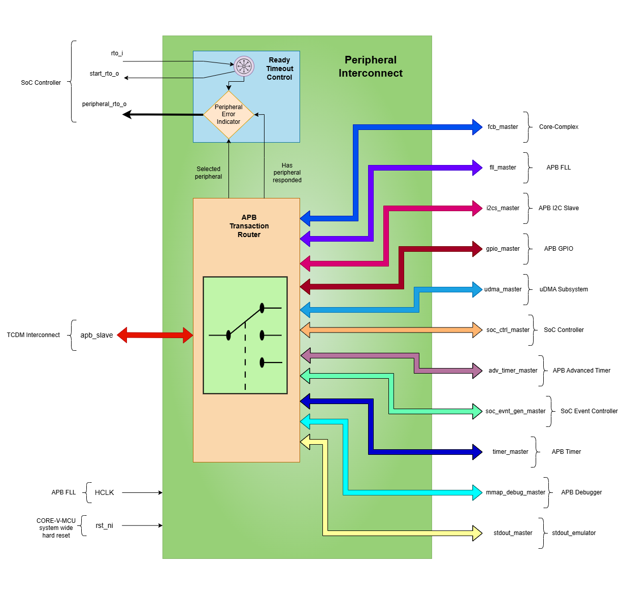
APB Peripheral Interconnect Block Diagram
APB Transaction Routing
The APB Peripheral Interconnect operates as a bridge between the TCDM Interconnect and multiple peripheral devices, allowing for efficient communication and data transfer. The APB transaction routing flow can be summarized as follows:
Firmware performs read/write operations to specific memory-mapped addresses, Core Complex initiates APB transactions to the APB Peripheral Interconnect via TCDM Interconnect.
The APB peripheral interconnect accepts the transaction coming from TCDM at the apb_slave interface.
- The APB Peripheral Interconnect provides routing to the following peripherals:
APB FLL
APB GPIO
uDMA Subsystem
APB SoC Controller
APB Advanced Timer
APB Event Controller
APB I2C Slave
APB Timer
eFPGA subsystem
APB Debugger
stdout emulator
APB Peripheral Interconnect routes these transactions received from TCDM interconnect to the peripherals based on address ranges and raises a start_rto_o signal to the SOC controller. Refer to the memory map for the complete address mapping of the peripherals.
APB Peripheral Interconnect uses the <peripheralName>_master (e.g., soc_ctrl_master, etc.) interface to forward the transaction to the peripherals.
Both master and slave interfaces of the APB peripheral are designed using the APB protocol.
If a peripheral fails to respond to APB interconnect within a predefined time i.e. the rto_i signal is asserted before the psel signal of the <peripheralName>_master interface, the integrated timeout detection mechanism activates and reports which peripheral has timed out. The timeout mechanism is discussed in the Timeout Mechanism section.
Timeout Mechanism
The APB Peripheral Interconnect includes a timeout detection mechanism to handle situations where a peripheral fails to respond within a specified time frame. Below is a description of the timeout handling process:
The start_rto_o signal is activated when a peripheral is selected based on the address specified in the APB transaction, triggering timeout counter in SoC Controller.
The SoC Controller has RTO_COUNT CSR that can be used to decide the timeout period. The default value of RTO_COUNT is 0xFF.
If a peripheral doesn’t respond within the timeout period i.e., the rto_i signal is asserted before the psel signal of the <peripheralName>_master interface, a timeout error occurs.
The SoC Controller deasserts the rto_i signal after one cycle.
When a timeout occurs, the peripheral_rto_o signals indicate which specific peripheral failed to respond, which then can be read through the SoC Controller’s RTO_PERIPHERAL CSR.(Check SoC Controller specs for more details)
The peripheral_rto_o signal is cleared after one clock cycle, i.e. once the rto_i signal has been deasserted.
The peripheral_rto_o signal to peripheral mapping can be found below:
Peripheral |
Index |
Default |
Description |
|---|---|---|---|
APB debugger |
10 |
0x0 |
1 indicates that the debugger interface caused a ready timeout |
stdout emulator |
9 |
0x0 |
1 indicates that the stdout emulator interface caused a ready timeout |
Core-Complex |
8 |
0x0 |
1 indicates that the FC/Core-Complex interface caused a ready timeout |
APB TIMER |
7 |
0x0 |
1 indicates that the Timer interface caused a ready timeout |
APB I2CS |
6 |
0x0 |
1 indicates that the I2CS interface caused a ready timeout |
APB EVENT CTRL |
5 |
0x0 |
1 indicates that the Event Controller interface caused a ready timeout |
APB ADV TIMER |
4 |
0x0 |
1 indicates that the Advanced Timer interface caused a ready timeout |
APB SOC CONTROL |
3 |
0x0 |
1 indicates that the SoC Controller interface caused a ready timeout |
uDMA subsystem |
2 |
0x0 |
1 indicates that the uDMA Subsystem interface caused a ready timeout |
APB GPIO |
1 |
0x0 |
1 indicates that the GPIO interface caused a ready timeout |
APB FLL |
0 |
0x0 |
1 indicates that the FLL interface caused a ready timeout |
System Architecture
The figure below depicts the connections between the CORE-V-MCU and rest of the modules in CORE-V-MCU:-
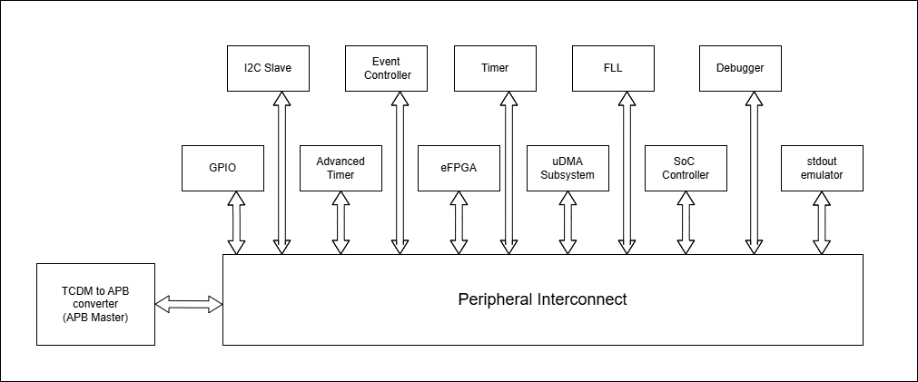
APB Peripheral Interconnect CORE-V-MCU connections diagram
Note: The stdout emulator is only used during simulation and does not correspond to an actual hardware block.
Firmware Guidelines
Since the APB Peripheral Interconnect is a memory-mapped peripheral, the firmware cannot access it directly. Although standard memory read/write operations to the APB peripheral devices will be routed through the Peripheral Interconnect.
The following general guidelines should be followed while interacting Peripheral devices through the APB Peripheral Interconnect:
Access peripheral registers using memory-mapped operations with the correct address calculated as (peripheral_base_address + register_offset).
Ensure that the firmware handles timeout conditions gracefully(Check SoC Controller specs for more details).
Implement error handling for cases where a peripheral does not respond within the expected time frame.
Pin Description
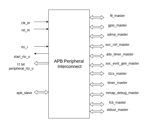
APB Peripheral Interconnect pin diagram
Clock and Reset Signals
clk_i: Input clock signal
rst_ni: Active-low reset signal
Ready Timeout Signals
rto_i: Input signal indicating a timeout condition from the SoC Controller
start_rto_o: Output signal indicating the start of a timeout condition
peripheral_rto_o [11:0]: Output signals indicating which peripheral has timed out
APB Slave Interface
apb_slave: APB slave interface, connected with TCDM Interconnect
APB Master Interfaces
fll_master: APB master interface for FLL
gpio_master: APB master interface for GPIO
udma_master: APB master interface for uDMA
soc_ctrl_master: APB master interface for SoC Controller
adv_timer_master: APB master interface for Advanced Timer
soc_evnt_gen_master: APB master interface for Event Generator
mmap_debug_master: APB master interface for Debugging
timer_master: APB master interface for Timer
fcb_master: APB master interface for eFPGA subsystem
stdout_master: APB master interface for Stdout, Not connected
i2cs_master: APB master interface for I2C Slave
Note: Each of the above master or slave interfaces has its own set of signals, including address, data, control, and ready signals, which are detailed below.
APB Interface Signals
PADDR[11:0]: APB address bus input
PWDATA[31:0]: APB write data bus input
PWRITE: APB write enable signal
PSEL: APB slave select input
PENABLE: APB enable signal
PRDATA[31:0]: APB read data bus output
PREADY: APB ready signal output, indicates completion of APB transaction
PSLVERR: APB slave error output