UDMA I2C Master
I²C (Inter-Integrated Circuit) is a multi-master, multi-slave, single-ended serial bus developed by Philips Semiconductor (now NXP Semiconductors), commonly used to connect lower-speed peripheral ICs to processors and microcontrollers. CORE-V-MCU CV32E40P (v1.0.0) has two I2C instances.
Features
Operates with two bi-directional open-drain lines; a Serial Data Line (SDA) and a Serial Clock Line (SCL), both pulled up with resistors.
Supports 7-bit or 10-bit address space, depending on the device.
Common bus speeds include 100 kbit/s (Standard mode) and 10 kbit/s (Low speed mode). Arbitrarily low clock frequencies are also allowed.
Architecture
uDMA I2C is a peripheral function of the uDMA subsystem. As such, its CSRs are not directly accessible via the APB bus. Rather, the control plane interface to the uDMA I2C is managed by the uDMA core within the uDMA subsystem. This is transparent to the programmer as all uDMA I2C CSRs appear within the uDMA Subsystem’s memory region. As is the case for all uDMA subsystem peripherals, I/O operations are controlled by the uDMA core. This is not transparent to the programmer.
The figure below is the high-level block diagram of the uDMA I2C:-
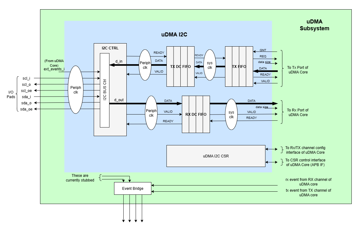
uDMA I2C Block Diagram
In the block diagram above, the DATA lines at the boundary of the uDMA I2C are 8 bits wide. The DATASIZE pin is 2 bits wide and is currently hardcoded to 0x0. The valid values for the DATASIZE pin are:
0x0: 1-byte transfer
0x1: 2-byte transfer
0x2: 4-byte transfer
The data from the TX DC FIFO, which is sent by uDMA Core, is first decoded by the I2C controller to determine whether it is a command or regular data (Refer to I2C controller state machine for detailed information). If it is identified as data, it is directly forwarded to the I2C bus controller. If it is a command, the I2C controller processes it by generating the appropriate control signals to I2C bus controller as specified by the command.
uDMA I2C uses the Tx channel interface to read the data from the interleaved (L2) memory via the uDMA Core. It transmits the read data to the external device. uDMA I2C uses the Rx channel interface to store the data received from the external device in interleaved (L2) memory. Refer to uDMA subsystem for more information about the Tx and Rx channel functionality of uDMA Core.
Dual clock FIFO
The uDMA core operates using the system clock, while the uDMA I2C operates using both the system clock and the peripheral clock. To ensure the uDMA I2C and core are properly synchronized, dual-clock FIFOs are used in the uDMA I2C. These are 4-depth FIFOs and can store 8-bit wide data. It is implemented using circular FIFO.
Below diagram shows the interfaces of DC FIFO:
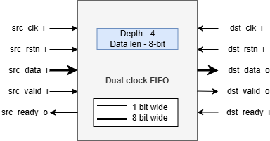
Dual clock FIFO
For Rx operation, source(src_*) interfaces shown in above diagram operate at peripheral clock and destination(dst_*) interfaces operate using system clock.
For Tx operation, source interfaces shown in above diagram operate at system clock and destination interfaces operate using peripheral clock.
Pop operation
The DC FIFO asserts the dst_valid_o (valid) signal to indicate that valid data is available on the data lines. A module waiting for data should read the data lines only when valid pin is high and drive the dst_ready_i (ready) signal to high and reset it in next clock cycle. When DC FIFO receives an active ready signal, indicating that the data has been read, it updates the data lines with new data if FIFO is not empty. If the FIFO is empty, the dst_valid_o signal is deasserted.
Push operation
The DC FIFO asserts the src_ready_o (ready) signal when there is available space to accept incoming data. When an active src_valid_i (valid) signal is received, the data is written into the FIFO. The src_ready_o signal is kept asserted as long as the FIFO has space for more data. IF the DC FIFO is full, push operation will be stalled until the FIFO has empty space and valid line is high. A module transmitting the data to DC FIFO should drive the valid signal low to indicate data lines should not be read.
During I2C transmit (Tx) operation, the TX DC FIFO is read internally by the I2C to transmit data to an external device and written by the TX FIFO. During I2C receive (Rx) operation, the RX DC FIFO is written internally by the I2C with the data received from the external device and read by the uDMA core.
TX FIFO
uDMA I2C has a TX FIFO to store the received data from uDMA core. It forwards the data read from L2 memory to the TX DC FIFO. uDMA I2C on TX path, read the data from TX DC FIFO and transmits it to external device. It is a 2-depth FIFO and can store 8-bit wide data. Below diagram shows the interfaces of TX FIFO:
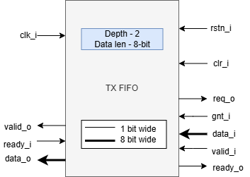
TX FIFO
TX FIFO operates using system clock. clr_i pin is hardcoded with value 0x0.
Pop operation
The read interface of the TX FIFO is connected to the TX DC FIFO. The TX DC FIFO raises ready(ready_i) signal if its FIFO has space. If data is available, TX FIFO asserts the valid_o signal and update the data lines with data. TX FIFO will update the valid signal and data lines at each clock cycle. If the ready signal is high, data lines will be update with new data, otherwise, data lines will show the last transferred byte. If the TX FIFO is empty, the valid_o signal remains deasserted, indicating that no valid data is present on the output lines.
Push operation
The write interface of the TX FIFO is extended to the uDMA Core. The TX FIFO write operation is performed with the help of the req(req_o) and ready(ready_o) signals. The TX FIFO keeps the ready_o (ready) signal high until the TX FIFO is full. TX FIFO raises a req_o signal when it has enough space in FIFO, i.e., ready_o is high, and the pending requests at the uDMA core do not exceed the depth of TX FIFO. TX FIFO receives a GNT (gnt_i) signal from the uDMA core confirming that the request is accepted. TX FIFO maintains a counter to track unserved requests; it applies the following logic to update the counter:-
When a request (req_o) is issued and granted (gnt_i), the TX FIFO increments the counter if either the valid_i or ready_o signal is low.
Regardless of the state of the req_o and gnt_i signals, the frame counter is decremented whenever both valid_i and ready_o are high.
When it receives the valid signal from the uDMA core and the FIFO is not full, the TX FIFO pushes the data coming from the uDMA core. TX tries to read data at each clock cycle until TX FIFO has space and a valid pin is high. TX FIFO is transparent to users.
I2C Controller
The I2C CTRL block implements the standard I2C protocol, responsible for managing all I2C bus operations such as start/stop condition generation, address transmission, data read/write, and acknowledgment handling. It receives data and command sequence from the uDMA interface via the TX path, decodes whether the incoming bytes is a command or data, and accordingly drives the necessary control signals to the I2C Bus controller for transmission over the I2C bus.
The I2C controller connects to the external I2C bus using two standard bidirectional lines:
SCL (Serial Clock Line): Carries the clock signal, generated by the I2C master to synchronize communication.
SDA (Serial Data Line): Carries the actual data between the master and slave devices.
I2C Command Encoding
The uDMA I2C controller executes I2C operations based on a set of command bytes written into L2 memory. Users are responsible to write command sequence into L2 memory before configuring I2C to perform TX/RX operations. It reads these commands into its internal TX FIFO via the uDMA core.
User must put the command in L2 memory in the correct sequence and format to implement valid I2C transactions. The controller automatically interprets and executes these commands upon receiving them through the uDMA interface.
Each command triggers a specific I2C action such as generating start/stop conditions, transmitting or receiving data, or configuring the clock.
The following table lists all supported commands and their encodings:
Encoding |
Command Name |
Command Description |
|---|---|---|
0x00 |
I2C_CMD_START |
Signals a start bit on the I2C bus |
0x10 |
I2C_WAIT_EV |
TBC: Inject wait states of data[1:0] in command buffer is non-zero |
0x20 |
I2C_CMD_STOP |
Signals a stop bit on the I2C bus |
0x40 |
I2C_CMD_RD_ACK |
Receives 1 byte and sends 1 acknowledge |
0x60 |
I2C_CMD_RD_NACK |
Receives 1 byte and sends 1 negative acknowledge |
0x80 |
I2C_CMD_WR |
Sends 1 byte and wait for acknowledge |
0xA0 |
I2C_CMD_WAIT |
The following byte indicates number of I2C cycles to wait |
0xC0 |
I2C_CMD_RPT |
The following byte indicates number of times to repeat next instruction |
0xE0 |
I2C_CMD_CFG |
Next two bytes are the MSB and LSB of the clock divider |
These command bytes must be issued in the correct sequence and format to implement valid I2C transactions. The controller automatically interprets and executes these commands upon receiving them through the uDMA interface.
I2C Operation flow
I2C communication always begins with a START and ends with a STOP, and can take the form of a single write, a single read, or a combined message (e.g., write immediately followed by a read). Regardless of the message types, all transfers can be decomposed into a small set of primitive operations:
Start Bit -> Send Byte and Get Acknowledge -> Get Byte and Send Acknowledge -> Get Byte and Sent Not Acknowledge -> Stop Bit
With different combinations of the above, we can create any type of I2C transfer. Under those conditions, the I2C IP interface is updated to fetch command from L2 memory instead of just transferring data. In this way we can recreate complex I2C transfer fully autonomously and without any intervention of the CPU.
Eg: Write and Read Operation
The following sequence illustrates a typical write followed by a read from an external I2C device. Commands are stored in the interleaved memory. When the Tx channel is enabled, the uDMA core transfers these commands to the uDMA I2C internal Tx buffer. Upon receiving the data, the I2C controller processes these commands as described below:
Command Issued |
Command Data |
Comment |
|---|---|---|
I2C_CMD_START |
Start the transfer |
|
I2C_CMD_WR |
0xA4 |
First byte: write to addr=0x52 |
I2C_CMD_RPT |
0x10 |
Repeat 16 times |
I2C_CMD_WR |
0x00, 0x01, 0x02, 0x3 |
|
0x04, 0x05, 0x06, 0x7 |
||
0x08, 0x09, 0x0A, 0xB |
||
0x0C, 0x0D, 0x0E, 0xF |
||
I2C_CMD_STOP |
Generate stop bits and end transfer |
|
I2C_CMD_WAIT |
0x10 |
Wait 16 I2C cycles |
I2C_CMD_START |
Start the next transfer |
|
I2C_CMD_WR |
0xA5 |
First byte: read from addr=0x52 |
I2C_CMD_RPT |
0x0F |
Repeat 15 times |
I2C_CMD_RD_ACK |
||
I2C_CMD_RD_NACK |
||
I2C_CMD_STOP |
We’re done! |
Transfer begins with I2C_CMD_START command, which generates a start bit on the bus.
The first byte sent following the I2C standard I2C_CMD_WR is 0xA4. This byte includes a 7-bit address (i.e., bits 1-7 of 0xA4) and 1-bit access type (i.e., bit 0 of 0xA4, where 0 - Write, 1 - read). Here 0xA4 is 8’b1010_0100, indicating a write operation to the address 7’b1010010 (i.e., 0x52).
The byte following the instruction I2C_CMD_RPT is 0x10, tells the number of times the next instruction has to be executed.
The next instruction I2C_CMD_WR is repeated 16 bytes and the data for each write instruction is queued. the 16 bytes of data to be written are: 0x00, 0x01, 0x02, …0x0F.
I2C_CMD_STOP generates the stop bits and ends the transfer.
I2C_CMD_WAIT waits for a defined number of I2C cycles (16 in this case) and after which I2C_CMD_START initiates a new I2C transfer.
The next command is a read from the same address. 0xA5 is sent, which corresponds to read from address 0x52 (same 7-bit address, with the LSB set to 1 for read).
The following I2C_CMD_RPT command repeats the I2C_CMD_RD_ACK, 15 times - this reads 15 bytes of data, sending an acknowledgment (ACK) after each byte.
The next command I2C_CMD_RD_NACK, reads the last byte and sends a not acknowledge (NACK) to signal the end of read operation.
I2C_CMD_STOP generates the stop bit and completes the transfer
All the commands/data are fetched through the Tx port from L2 memory into I2C Tx buffer, while the incoming read data is pushed into I2C Rx buffer.
TX Operation
To transmit data to an external I2C device, the uDMA I2C must be configured using the TX_SADDR, TX_SIZE and TX_CFG CSRs. The transfer proceeds in three stages:-
Fetching data from L2 memory into TX FIFO
The TX FIFO requests data from the uDMA core by asserting both the READY (space available) and REQ (request a new transaction) signals. The uDMA core arbitrates among multiple peripherals on receiving the REQ signal. When the I2C TX channel is enabled and wins arbitration, the uDMA core issues a GNT (grant) signal and places the valid data read from L2 memory on the bus along with asserting VALID signal. Tx FIFO stores this received data and keeps the READY and REQ signals asserted as long as the aforementioned conditions remain valid. The uDMA core de-asserts the VALID signal in the following clock cycle and reasserts it only when new data is available for transmission. Initially, after reset or power-up, READY/REQ are asserted since the FIFO is empty.
Transferring data from TX FIFO to TX DC FIFO
The TX DC FIFO asserts READY signal when it can accept data. Whenever TX FIFO has valid data, it asserts VALID signal and update the data lines of DC FIFO with the valid data. The data transmission from TX FIFO to TX DC FIFO is synchronized using system clock. TX DC FIFO de-asserts READY when it is full, temporarily stalling the upstream TX FIFO. Once space is freed, READY is re-asserted. Data moves from TX FIFO to TX DC FIFO when both VALID and READY are high on the same cycle.
Consuming data from DC TX FIFO
The I2C controller asserts READY when it can accept data and continuously monitors the TX DC FIFO. When VALID is asserted, it latches the data into a local variable and immediately de-asserts READY , processes the byte and re-asserts READY when ready for next. Each byte is interpreted as either a command or data:
Write commands - following data bytes are sent to the external device over the I2C bus.
Read command - trigger the I2C controller to read the data from the external device over the I2C bus and push it into the internal RX DC FIFO, from where it can be retrieved later by the uDMA core.
The cycle continues until the entire programmed transfer length is executed, ensuring autonomous command execution of I2C transfers.
RX Operation
Unlike a pure write transaction, reading data from an I2C slave requires a two-step process:
Issuing a Read Command (via TX path)
Before any data can be received from external device, TX channels must be configured such that read command sequence can be fetched from L2 memory (same as described above in Tx Operation). The I2C controller then performs the corresponding bus transactions, retrieving data bytes from the addressed slave device.
NOTE: Without this initial TX transaction, no data will be placed on the bus by the slave.
Transfer Data to L2 Memory
Once the read command is acknowledged, the I2C controller shift in data bytes from the slave device. Each received bytes is pushed into the RX DC FIFO, and the FIFO asserts VALID to indicate the availability of new data.
To store the received data into L2 memory, the uDMA I2C must be programmed with RX_SADDR, RX_SIZE and RX_CFG CSRs.
On detecting the valid signal, the uDMA core arbitrates for access. If the uDMA I2C RX channel wins the arbitration and the core’s RX FIFO has space, uDMA core asserts READY, latching the data from RX DC FIFO. The data is then written into L2 memory at the address specified by RX_SADDR, wih automatic increment for subsequent bytes. The cycle repeats until the entire transfer (as defined by RX_SIZE) completes.
System Architecture
The figure below shows how the uDMA I2C interfaces with the rest of the CORE-V-MCU components and the external I2C Slave device:-
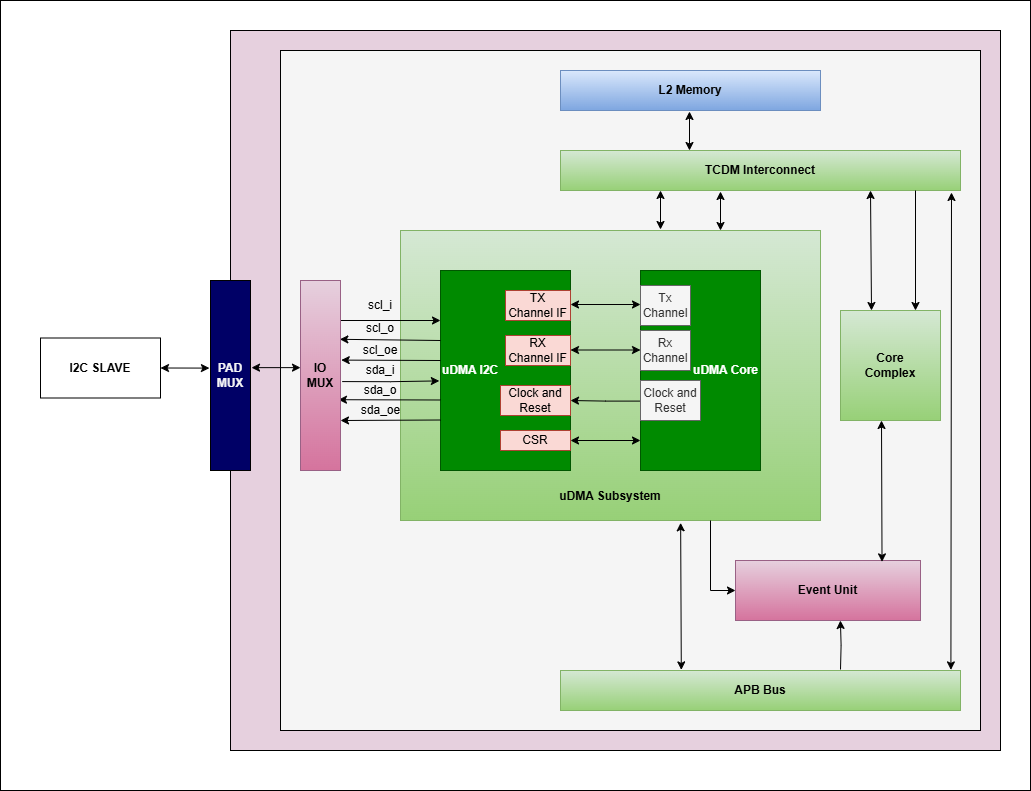
uDMA I2C CORE-V-MCU Connection Diagram
Programming Model
As with most peripherals in the uDMA Subsystem, software configuration for the I²C interface can be conceptualized into three key steps:
I/O Configuration - Set up SDA/SCL pins, clock frequency, and addressing mode. This prepares the I²C interface for communication.
uDMA Setup - Configure source/destination addresses, transfer size, and direction using TX and RX channel CSRs. This enables efficient data movement from L2 memory to I2C via uDMA core. Update the L2 memory with command sequence to configure I2C controller.
Data Transfer Management - Read command sequence from L2 memory to configure I2C for RX/TX operation. Drive I2C bus based on the commands. Monitor the status using STATUS CSR and reset via SETUP CSR, when needed.
Data Transfer Operation
Refer to the Firmware Guidelines section in the current chapter
UDMA I2CM CSRs
Refer to Memory Map for peripheral domain address of the uDMA I2C0 and uDMA I2C1.
NOTE: Several of the uDMA I2C CSR are volatile, meaning that their read value may be changed by the hardware. For example, writing to RX_SADDR CSR will set the address of the receive buffer pointer. As data is received, the hardware will update the value of the pointer to indicate the current address. As the name suggests, the value of non-volatile CSRs is not changed by the hardware. These CSRs retain the last value written by software.
A CSRs volatility is indicated by its “type”.
Details of CSR access type are explained here .
The CSR’s RX_SADDR, RX_SIZE specifies the configuration for the transaction on the RX channel. The CSR’s TX_SADDR, TX_SIZE specify the configuration for the transaction on the TX channel. The uDMA Core creates a local copy of this information at its end and use it for current ongoing transaction.
RX_SADDR
Offset: 0x0
Type : Volatile
Field |
Bits |
Type |
Default |
Description |
|---|---|---|---|---|
SADDR |
11:0 |
RW |
0x0 |
Address of Rx buffer on write. This is the address of L2 memory where I2C will write the received data. Read & write to this CSR access different information. On Write: Address of Rx buffer for next transaction. It does not impact current ongoing transaction. On Read: Address of Rx buffer for the current ongoing transaction. This is the local copy of information maintained inside the uDMA Core. |
RX_SIZE
Offset: 0x04
Type : Volatile
Field |
Bits |
Type |
Default |
Description |
|---|---|---|---|---|
SIZE |
15:0 |
RW |
0x0 |
Size of Rx buffer (amount of data to be transferred by I2C to L2 memory). Read & write to this CSR access different information. On Write: Size of Rx buffer for next transaction. It does not impact current ongoing transaction. On Read: Bytes left for the current ongoing transaction i.e., bytes left to write to L2 memory. This is the local copy of information maintained inside the uDMA Core. |
RX_CFG
Offset: 0x08
Type : Volatile
Field |
Bits |
Type |
Default |
Description |
|---|---|---|---|---|
CLR |
6:6 |
WO |
0x0 |
Clear the local copy of Rx channel configuration CSRs inside uDMA core |
PENDING |
5:5 |
RO |
0x0 |
|
EN |
4:4 |
RW |
0x0 |
Enable the Rx channel of uDMA core to perform Rx Operation |
CONTINUOUS |
0:0 |
RW |
0x0 |
|
TX_SADDR
Offset: 0x10
Type : Volatile
Field |
Bits |
Type |
Default |
Description |
|---|---|---|---|---|
SADDR |
11:0 |
RW |
0x0 |
Address of Tx buffer on write. This is the address of L2 memory from where I2C will read the data to transmit. Read & write to this CSR access different information. On Write: Address of Tx buffer for next transaction. It does not impact current ongoing transaction. On Read: Address of Tx buffer for the current ongoing transaction. This is the local copy of information maintained inside the uDMA Core. |
TX_SIZE
Offset: 0x14
Type : Volatile
Field |
Bits |
Type |
Default |
Description |
|---|---|---|---|---|
SIZE |
15:0 |
RW |
0x0 |
Size of Tx buffer (amount of data to be read by I2C from L2 memory). Read & write to this CSR access different information. On Write: Size of Tx buffer for next transaction. It does not impact current ongoing transaction. On Read: Bytes left for the current ongoing transaction i.e., bytes left to read from L2 memory. This is the local copy of information maintained inside the uDMA Core. |
TX_CFG
Offset: 0x18
Type : Volatile
Field |
Bits |
Type |
Default |
Description |
|---|---|---|---|---|
CLR |
6:6 |
WO |
0x0 |
Clear the local copy of Tx channel configuration CSRs inside uDMA core |
PENDING |
5:5 |
RO |
0x0 |
|
EN |
4:4 |
RW |
0x0 |
Enable the transmit channel of uDMA core to perform Tx operation |
CONTINUOUS |
0:0 |
RW |
0x0 0x0 |
|
STATUS
Offset: 0x20
Type : Volatile
Field |
Bits |
Type |
Default |
Description |
|---|---|---|---|---|
AL |
1:1 |
RO |
0x0 |
Always returns 0 |
BUSY |
0:0 |
RO |
0x0 |
Always returns 0 |
NOTE: No functionality is implemented in RTL and always returns 0x0.
SETUP
Offset: 0x24
Type : Volatile
Field |
Bits |
Type |
Default |
Description |
|---|---|---|---|---|
RESET |
0:0 |
RW |
0x0 |
Issues a soft reset to the I2C controller, aborting any ongoing transactions. |
Firmware Guidelines
Clock Enable, Rest uDMA I2C
Configure the uDMA Core’s PERIPH_CLK_ENABLE CSR to enable uDMA I2C’s peripheral clock.
Set the uDMA Core’s PERIPH_RESET CSR to issue a soft reset signal to uDMA I2C, which clear CSRs and aborts ongoing transactions.
Set the uDMA I2C’s SETUP CSR to issue a soft reset signal to uDMA I2C controller to abort any ongoing transactions.
NOTE: Setting the uDMA Core’s PERIPH_RESET CSR aborts ongoing transactions and clears all I2C CSRs. In contrast, setting the uDMA I2C’s SETUP CSR aborts only the ongoing transactions, without affecting its CSRs.
Tx Operation (Read from L2 memory)
Configure the uDMA I2C’s TX_SADDR CSR with an interleaved(L2) memory address where the I2C configuration commands and Tx data is stored. I2C will read the data from this memory address.
Set the uDMA I2C’s TX_SIZE CSR to specify the amount of data (in bytes) to be transferred/read from the L2 memory address provided in TX_SADDR.
Configure uDMA I2C’s TX_CFG CSR to enable the Tx channel, which allows the Tx channel to start reading data.
The completion of the Tx operation can be determined by reading the TX_SIZE CSR. A value of 0 indicates that there are no pending bytes remaining for transfer.
Rx Operation (Write to L2 memory)
To enable RX operation , the TX channel must first be configured to read the I2C configuration details from L2 memory. Refer to the above section Tx Operation (Read from L2 memory)
Note: After the I2C controller fetches the configuration and performs a read operation from the slave device, the received data is first stored in an internal FIFO buffer. To transfer this data to L2 memory, the Rx channel must be configured as described below:
Configure the uDMA I2C’s RX_SADDR CSR with an interleaved(L2) memory address where the data will be written. I2C will write the data to this memory address.
Set the uDMA I2C’s RX_SIZE CSR to specify the amount of data (in bytes) to be transferred/written to the L2 memory address provided in RX_SADDR.
Configure uDMA I2C’s RX_CFG CSR to enable the Rx channel, which allows the Rx channel to start writing the data.
The completion of the Rx operation can be determined by reading the RX_SIZE CSR. A value of 0 indicates that there are no pending bytes remaining for transfer.
Pin Diagram
The figure below is the pin diagram of the uDMA I2C
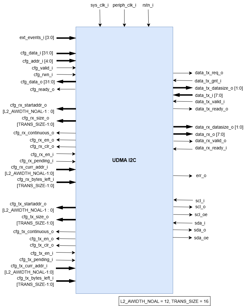
uDMA I2C Pin Diagram
Below is the categorization of the pins:
Tx Channel Interface
The following pins constitute the Tx channel interface of uDMA I2C. These pins are used to read the data from interleaved (L2) memory:
data_tx_req_o: Read request signal.data_tx_gnt_i: Read grant signal.data_tx_datasize_o [1:0]: Data size for Tx channel.data_tx_i [7:0]: Data input for Tx channel.data_tx_valid_i: Valid data input signal.data_tx_ready_o: Tx ready output signal.
Rx Channel Interface
The following pins constitute the Rx channel interface of uDMA I2C. These pins are used to write the data to interleaved (L2) memory:
data_rx_datasize_o [1:0]: Data size for Rx channel.data_rx_o [7:0]: Data output for Rx channel.data_rx_valid_o: Valid data output signal.data_rx_ready_i: Rx ready input signal.
uDMA I2C interface to get/send data from/to external device
scl_i: I2C clock input signal.scl_o: I2C clock output signal.scl_oe: Output enable for clock line.sda_i: I2C data input signal.sda_o: I2C data output.sda_oe: Output enable for data line
uDMA I2C interface to read-write CSRs
The following interfaces are used to read and write to I2C CSRs. These interfaces are managed by uDMA Core.
cfg_data_i [31:0]: APB Write data.cfg_addr_i [4:0]: APB Address.cfg_valid_i: APB data valid signal.cfg_rwn_i: APB read or write signal.cfg_data_o [31:0]: APB read data output.cfg_ready_o: APB ready signal.
uDMA I2C Tx channel configuration interface
uDMA I2C uses these pins to share TX_SADDR, TX_SIZE and TX_CFG CSR details with core:
cfg_tx_startaddr_o: Start address configuration output.cfg_tx_size_o: Transfer size configuration output.cfg_tx_continuous_o: Continuous transfer mode enable signal.cfg_tx_en_o: Tx channel enable configuration output.cfg_tx_clr_o: Clear config signal for Tx.
uDMA I2C shares the values of the below pins as read values of TX_SADDR, TX_SIZE and TX_CFG CSR:
cfg_tx_en_i: Enable signal for Tx channel.cfg_tx_pending_i: Tx pending status input.cfg_tx_curr_addr_i: Current address being written to.cfg_tx_bytes_left_i: Bytes remaining to transmit.
uDMA I2C Rx channel configuration interface
uDMA I2C uses these pins to share RX_SADDR, RX_SIZE and RX_CFG CSR details with core:
cfg_rx_startaddr_o: Start address configuration output.cfg_rx_size_o: Transfer size configuration output.cfg_rx_continuous_o: Continuous transfer mode enable signal.cfg_rx_en_o: Rx channel enable configuration output.cfg_rx_clr_o: Clear config signal for Rx.
uDMA I2C shares the values of the below pins as read values of RX_SADDR, RX_SIZE and RX_CFG CSR:
cfg_rx_en_i: Enable signal for Rx channel.cfg_rx_pending_i: rx pending status input.cfg_rx_curr_addr_i: Current address being read from.cfg_rx_bytes_left_i: Bytes remaining to left.
Clock interface
These pins are used to synchronize I2C with uDMA core.
sys_clk_i: System clock.periph_clk_i: Peripheral clock.
Reset interface
uDMA core issues reset signal to I2C via this pin.
rstn_i: soft reset signal enabled through the uDMA core CSR.
External events
uDMA core triggers these events based on specific conditions. The I2C will only wait for these events when I2C_WAIT_EV command is issued.
ext_events_i [3:0]: Input external events.
uDMA I2C interface to generate error
err_o
**Note**:: As of commit #30e3c8b, the err_o signal is left unconnected.