eFPGA SubSystem
This is the eFPGA subsystem from QuickLogic. Based on ArcticPro 2 architecture Silicon-verified, production-proven eFPGA for MCU/SoC/custom ASIC applications - optimized for edge and endpoint AI processing, military and automotive. QuickLogic has been supplying eFPGA-based products for consumer, industrial and mission-critical applications for nearly three decades. Our eFPGA IP enables SoC designers the flexibility to easily program custom functions, hardware accelerators and security capability after an SoC has been manufactured.
Subsystem Architecture
The eFPGA block is an array of 32x32 SLC’s (Super Logic Cells), each SLC is composed of 2 LUT5s and 4 LUT4s
eFPGA Subsystem Components
Functional Description
Logic Cell
The eFPGA block
Math Units
The EFPGA has 2 Math units attached. Each math unit has 3 block RAMS (4KBytes) and 2 Multipliers. Each Block RAM has one read port and one write port with independant clocks. Each Port can be independenly configured as 8-bit, 16-bit or 32-bit by the configuration on the appropriate rmode, or wmode inputs. The Write data can also be selected to be from the fabric or the output of the Associated Multiplier.
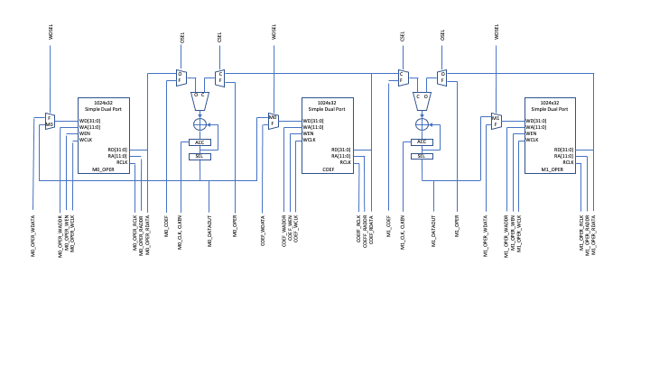
Block RAM
Clocking
The eFPGA recieves 6 clocks from the SOC.
Clk0 is sourced by the PLL and the eFPGA divisor Circuit.
CLK1 is sources by the PLL and the peripheral divisor Circuit.
CLK2 is sourced by the RefClock divisor Circut.
CLK3 is source by an IO pin.
CLK4 is sourced by an IO pin.
CLK5 is sourced by an IO pin.
SoC Interfaces
Configurable Input/Output Signals
The example RTL file top.sv in the rtl/simulation folder is functional rtl design for verifying the eFPGA interfaces. It contain the mapping from the eFPGA to the SoC and IO. The example design instantiates all the interfaces and has simple logic that allows for exercising the interfaces, The various registers allow for control of all the resources and interfaces with simple state machines to demostrate the use of the resources.
L2 Interface
The L2 interface to the eFPGA is a memory mapped interface that is allocated a 1Mbyte address space. It is asynchronous to the CPU and contains clock crossing registers to maintain data integrity. the following table contains the L2 Interface signals. Various control registers are accessible via the L2 interface to test other functions in the eFPGA.
direction |
Name |
Description. |
|---|---|---|
input |
lint_REQ |
Cycle request active high |
input |
lint_WEN |
Write = 1, Read = 0. |
input |
lint_ADDR[19:0] |
Address 20-bits |
input |
lint_WDATA[31:0] |
Write Data 32-bits |
input |
lint_BE[3:0] |
Byte enables 4-bits. |
output |
lint_VALID |
Valid signal (ack) |
output |
lint_GNT |
Grant signal |
output |
lint_RDATA[31:0] |
Read Data 32-bits |
output |
lint_clk |
Clock back to CDC logic |
TCDM Interface
Core-v-mcu provides 4 TCDM (Tightly Coupled Distributed memory) Each of the these interfaces has full access to the 512KB of SoC memory allowing the eFPGA to perform reads and writes to memory. Each interface is connected through Clock Domain Crossing registers as the eFPGA is clocked by asynchronously from the SoC.
Direction |
Name |
Description |
|---|---|---|
output |
tcdm_addr_p0[19:0] |
20-bit address for TCDM |
input |
tcdm_rdata_p0[31:0] |
32-bit Read data returned from TCDM |
input |
tcdm_valid_p0 |
TCDM read data Valid |
input |
tcdm_gnt_p0 |
TCDM Grant indicating the cycle is in progress |
input |
tcdm_fmo_p0 |
TCDM interface can accept only one more request |
output |
tcdm_wdata_p0[31:0] |
32-bit Data to write to TCDM |
output |
tcdm_be_p0[3:0] |
4 byte enables for byte writes |
output |
tcdm_wen_p0 |
Write enable active high |
output |
tcdm_req_p0 |
TCDM cycle request |
output |
tcdm_clk_p0 |
TCDM clock from eFPGA to CDC logic |
eFPGA Subsystem Registers
The eFPGA Template instantiates all the user accessible IO in the eFPGA and makes it available for logic validation .
The eFPGA provide the following interfaces and resources 1. Asynchronous CPU read/write bus. With 32-bit data, byte enables and 20-bits Address 2. Four TCDM interfaces for eFPGA high speed access to read/write main L2 RAM 3. 32-bits of fpga IO which connects the fpga to the device pins via the pin mux 4. 16-bits of event generation that can interrupt the CPU. 5. 2 Math units each mathunit contains 2 32-bit multipliers that can be fractured into 2-16-bit, 4-8-bit or 8-4-bit multiply with accumulators and 3 4Kbyte Simple dual port RAMS.
TCDM_CTL_P0 offset = 0x00
Field |
Bits |
Type |
Default |
Description |
|---|---|---|---|---|
tcdm_wen_p0 |
31:31 |
RW |
0x0 |
1 = read on TCDM 0, 0 = write on TCDM 0 |
tcdm_be_p0 |
23:20 |
RW |
0x0 |
Set the bye enables for TCDM 0 |
tcdm_addr_p0 |
19:0 |
RW |
0x0 |
Sets the address to be used on TCDM 0 |
TCDM_CTL_P1 offset = 0x04
Field |
Bits |
Type |
Default |
Description |
|---|---|---|---|---|
tcdm_wen_p1 |
31:31 |
RW |
0x0 |
1 = read on TCDM 1, 0 = write on TCDM 1 |
tcdm_be_p1 |
23:20 |
RW |
0x0 |
Set the bye enables for TCDM 1 |
tcdm_addr_p1 |
19:0 |
RW |
0x0 |
Sets the address to be used on TCDM 1 |
TCDM_CTL_P2 offset = 0x08
Field |
Bits |
Type |
Default |
Description |
|---|---|---|---|---|
tcdm_wen_p2 |
31:31 |
RW |
0x0 |
1 = read on TCDM 2, 0 = write on TCDM 2 |
tcdm_be_p2 |
23:20 |
RW |
0x0 |
Set the bye enables for TCDM 2 |
tcdm_addr_p2 |
19:0 |
RW |
0x0 |
Sets the address to be used on TCDM 2 |
TCDM_CTL_P3 offset = 0x0C
Field |
Bits |
Type |
Default |
Description |
|---|---|---|---|---|
tcdm_wen_p3 |
31:31 |
RW |
0x0 |
1 = read on TCDM 3, 0 = write on TCDM 3 |
tcdm_be_p3 |
23:20 |
RW |
0x0 |
Set the bye enables for TCDM 3 |
tcdm_addr_p3 |
19:0 |
RW |
0x0 |
Sets the address to be used on TCDM 3 |
There are 4 control regsisters (1 for each of te multiplier units) the bits in these registers will configure the multipler operation.
M0_M0_CONTROL offset = 0x10
Field |
Bits |
Type |
Default |
Description |
|---|---|---|---|---|
m0_m0_reset |
31:31 |
RW |
0x0 |
Math Unit 0, Multiplier 0 reset accumulator |
m0_m0_sat |
18:18 |
RW |
0x0 |
Math Unit 0, Multiplier 0 select saturation |
m0_m0_clr |
17:17 |
RW |
0x0 |
Math Unit 0, Multiplier 0 clear accumulator |
m0_m0_rnd |
16:16 |
RW |
0x0 |
Math Unit 0, Multiplier 0 select rounding |
m0_m0_csel |
15:15 |
RW |
0x0 |
Math Unit 0, Multiplier 0 coefficient selection |
m0_m0_osel |
14:14 |
RW |
0x0 |
Math Unit 0, Multiplier 0 operand slection |
m0_m0_mode |
13:12 |
RW |
0x0 |
Math Unit 0, Multiplier 0 mode. 00 = 32-bit, 01 = 16-bit, 10= 8-bit, 11 = 4-bit |
m0_m0_outsel |
5:0 |
RW |
0x0 |
Math Unit 0, Mutliplier 0 output select |
M0_M1_CONTROL offset = 0x14
Field |
Bits |
Type |
Default |
Description |
|---|---|---|---|---|
m0_m1_reset |
31:31 |
RW |
0x0 |
Math Unit 0, Multiplier 1 reset accumulator |
m0_m1_sat |
18:18 |
RW |
0x0 |
Math Unit 0, Multiplier 1 select saturation |
m0_m1_clr |
17:17 |
RW |
0x0 |
Math Unit 0, Multiplier 1 clear accumulator |
m0_m1_rnd |
16:16 |
RW |
0x0 |
Math Unit 0, Multiplier 1 select rounding |
m0_m1_csel |
15:15 |
RW |
0x0 |
Math Unit 0, Multiplier 1 coefficient selection |
m0_m1_osel |
14:14 |
RW |
0x0 |
Math Unit 0, Multiplier 1 operand slection |
m0_m1_mode |
13:12 |
RW |
0x0 |
Math Unit 0, Multiplier 1 mode. 00 = 32-bit, 01 = 16-bit, 10= 8-bit, 11 = 4-bit |
m0_m1_outsel |
5:0 |
RW |
0x0 |
Math Unit 0, Mutliplier 1 output select |
M1_M0_CONTROL offset = 0x18
Field |
Bits |
Type |
Default |
Description |
|---|---|---|---|---|
m1_m0_reset |
31:31 |
RW |
0x0 |
Math Unit 1, Multiplier 0 reset accumulator |
m1_m1_sat |
18:18 |
RW |
0x0 |
Math Unit 1, Multiplier 0 select saturation |
m1_m0_clr |
17:17 |
RW |
0x0 |
Math Unit 1, Multiplier 0 clear accumulator |
m1_m0_rnd |
16:16 |
RW |
0x0 |
Math Unit 1, Multiplier 0 select rounding |
m1_m0_csel |
15:15 |
RW |
0x0 |
Math Unit 1, Multiplier 0 coefficient selection |
m1_m0_osel |
14:14 |
RW |
0x0 |
Math Unit 1, Multiplier 0 operand slection |
m1_m0_mode |
13:12 |
RW |
0x0 |
Math Unit 1, Multiplier 0 mode. 00 = 32-bit, 01 = 16-bit, 10= 8-bit, 11 = 4-bit |
m1_m0_outsel |
5:0 |
RW |
0x0 |
Math Unit 1, Mutliplier 0 output select |
M1_M1_CONTROL offset = 0x1C
Field |
Bits |
Type |
Default |
Description |
|---|---|---|---|---|
m1_m1_reset |
31:31 |
RW |
0x0 |
Math Unit 1, Multiplier 1 reset accumulator |
m1_m1_sat |
18:18 |
RW |
0x0 |
Math Unit 1, Multiplier 1 select saturation |
m1_m1_clr |
17:17 |
RW |
0x0 |
Math Unit 1, Multiplier 1 clear accumulator |
m1_m1_rnd |
16:16 |
RW |
0x0 |
Math Unit 1, Multiplier 1 select rounding |
m1_m1_csel |
15:15 |
RW |
0x0 |
Math Unit 1, Multiplier 1 coefficient selection |
m1_m1_osel |
14:14 |
RW |
0x0 |
Math Unit 1, Multiplier 1 operand slection |
m1_m1_mode |
13:12 |
RW |
0x0 |
Math Unit 1, Multiplier 1 mode. 00 = 32-bit, 01 = 16-bit, 10= 8-bit, 11 = 4-bit |
m1_m1_outsel |
5:0 |
RW |
0x0 |
Math Unit 1, Mutliplier 1 output select |
Two RAM control registers are provide to configure the RAMs (1 for each Math unit)
M0_RAM_CONTROL offset = 0x20
Field |
Bits |
Type |
Default |
Description |
|---|---|---|---|---|
m0_coef_wdsel |
14:14 |
RW |
0x0 |
Math Unit 0 coefficient RAM write data select 0 = Fabric, 1 = Multipler output |
m0_oper1_wdsel |
13:13 |
RW |
0x0 |
Math Unit 0 Operand 0 RAM write data select 0 = Fabric, 1 = Multipler output |
m0_oper0_wdsel |
12:12 |
RW |
0x0 |
Math Unit 0 Operand 1 RAM write data select 0 = Fabric, 1 = Multipler output |
m0_coef_wmode |
11:10 |
RW |
0x0 |
Math Unit 0 coefficient RAM write mode 00 = 32-bit, 01 = 16=bit 10 = 8=bit |
m0_coef_rmode |
9:8 |
RW |
0x0 |
Math Unit 0 coefficient RAM read mode 00 = 32-bit, 01 = 16=bit 10 = 8=bit |
m0_oper1_wmode |
7:6 |
RW |
0x0 |
Math Unit 0 operand 0 RAM write mode 00 = 32-bit, 01 = 16=bit 10 = 8=bit |
m0_oper1_rmode |
5:4 |
RW |
0x0 |
Math Unit 0 operand 0 RAM read mode 00 = 32-bit, 01 = 16=bit 10 = 8=bit |
m0_oper0_wmode |
3:2 |
RW |
0x0 |
Math Unit 0 operand 1 RAM write mode 00 = 32-bit, 01 = 16=bit 10 = 8=bit |
m0_oper0_rmode |
1:0 |
RW |
0x0 |
Math Unit 0 operand 1 RAM read mode 00 = 32-bit, 01 = 16=bit 10 = 8=bit |
M1_RAM_CONTROL offset = 0x24
Field |
Bits |
Type |
Default |
Description |
|---|---|---|---|---|
m1_coef_wdsel |
14:14 |
RW |
0x0 |
Math Unit 1 coefficient RAM write data select 0 = Fabric, 1 = Multipler output |
m1_oper1_wdsel |
13:13 |
RW |
0x0 |
Math Unit 1 Operand 0 RAM write data select 0 = Fabric, 1 = Multipler output |
m1_oper0_wdsel |
12:12 |
RW |
0x0 |
Math Unit 1 Operand 1 RAM write data select 0 = Fabric, 1 = Multipler output |
m1_coef_wmode |
11:10 |
RW |
0x0 |
Math Unit 1 coefficient RAM write mode 00 = 32-bit, 01 = 16=bit 10 = 8=bit |
m1_coef_rmode |
9:8 |
RW |
0x0 |
Math Unit 1 coefficient RAM read mode 00 = 32-bit, 01 = 16=bit 10 = 8=bit |
m1_oper1_wmode |
7:6 |
RW |
0x0 |
Math Unit 1 operand 0 RAM write mode 00 = 32-bit, 01 = 16=bit 10 = 8=bit |
m1_oper1_rmode |
5:4 |
RW |
0x0 |
Math Unit 1 operand 0 RAM read mode 00 = 32-bit, 01 = 16=bit 10 = 8=bit |
m1_oper0_wmode |
3:2 |
RW |
0x0 |
Math Unit 1 operand 1 RAM write mode 00 = 32-bit, 01 = 16=bit 10 = 8=bit |
m1_oper0_rmode |
1:0 |
RW |
0x0 |
Math Unit 1 operand 1 RAM read mode 00 = 32-bit, 01 = 16=bit 10 = 8=bit |
Four clock enable registers that are write only and clear to zero, when written to a ‘1’ and single clock enable will be generated to the specified multiplier.
M0_M0_CLKEN offset = 0x30
Field |
Bits |
Type |
Default |
Description |
|---|---|---|---|---|
m0_m0_clken |
0:0 |
WO |
Math Unit 0 Multiplier 0 Clock enable |
M0_M1_CLKEN offset = 0x34
Field |
Bits |
Type |
Default |
Description |
|---|---|---|---|---|
m0_m1_clken |
0:0 |
WO |
Math Unit 0 Multiplier 1 Clock enable |
M1_M0_CLKEN offset = 0x38
Field |
Bits |
Type |
Default |
Description |
|---|---|---|---|---|
m1_m0_clken |
0:0 |
WO |
Math Unit 1 Multiplier 0 Clock enable |
M1_M1_CLKEN offset = 0x3C
Field |
Bits |
Type |
Default |
Description |
|---|---|---|---|---|
m1_m1_clken |
0:0 |
WO |
Math Unit 1 Multiplier 1 Clock enable |
FPGAIO_OUT31_00 offset = 0x40
Field |
Bits |
Type |
Default |
Description |
|---|---|---|---|---|
fpgaio_o_31 |
31:31 |
RW |
0x0 |
Sets the fpgio output bit 31 |
fpgaio_o_30 |
30:30 |
RW |
0x0 |
Sets the fpgio output bit 30 |
fpgaio_o_29 |
29:29 |
RW |
0x0 |
Sets the fpgio output bit 29 |
fpgaio_o_28 |
28:28 |
RW |
0x0 |
Sets the fpgio output bit 28 |
fpgaio_o_27 |
27:27 |
RW |
0x0 |
Sets the fpgio output bit 27 |
fpgaio_o_26 |
26:26 |
RW |
0x0 |
Sets the fpgio output bit 26 |
fpgaio_o_25 |
25:25 |
RW |
0x0 |
Sets the fpgio output bit 25 |
fpgaio_o_24 |
24:24 |
RW |
0x0 |
Sets the fpgio output bit 24 |
fpgaio_o_23 |
23:23 |
RW |
0x0 |
Sets the fpgio output bit 23 |
fpgaio_o_22 |
22:22 |
RW |
0x0 |
Sets the fpgio output bit 22 |
fpgaio_o_21 |
21:21 |
RW |
0x0 |
Sets the fpgio output bit 21 |
fpgaio_o_20 |
20:20 |
RW |
0x0 |
Sets the fpgio output bit 20 |
fpgaio_o_19 |
19:19 |
RW |
0x0 |
Sets the fpgio output bit 19 |
fpgaio_o_18 |
18:18 |
RW |
0x0 |
Sets the fpgio output bit 18 |
fpgaio_o_17 |
17:17 |
RW |
0x0 |
Sets the fpgio output bit 17 |
fpgaio_o_16 |
16:16 |
RW |
0x0 |
Sets the fpgio output bit 16 |
fpgaio_o_15 |
15:15 |
RW |
0x0 |
Sets the fpgio output bit 15 |
fpgaio_o_14 |
14:14 |
RW |
0x0 |
Sets the fpgio output bit 14 |
fpgaio_o_13 |
13:13 |
RW |
0x0 |
Sets the fpgio output bit 13 |
fpgaio_o_12 |
12:12 |
RW |
0x0 |
Sets the fpgio output bit 12 |
fpgaio_o_11 |
11:11 |
RW |
0x0 |
Sets the fpgio output bit 11 |
fpgaio_o_10 |
10:10 |
RW |
0x0 |
Sets the fpgio output bit 10 |
fpgaio_o_9 |
9:9 |
RW |
0x0 |
Sets the fpgio output bit 9 |
fpgaio_o_8 |
8:8 |
RW |
0x0 |
Sets the fpgio output bit 8 |
fpgaio_o_7 |
7:7 |
RW |
0x0 |
Sets the fpgio output bit 7 |
fpgaio_o_6 |
6:6 |
RW |
0x0 |
Sets the fpgio output bit 6 |
fpgaio_o_5 |
5:5 |
RW |
0x0 |
Sets the fpgio output bit 5 |
fpgaio_o_4 |
4:4 |
RW |
0x0 |
Sets the fpgio output bit 4 |
fpgaio_o_3 |
3:3 |
RW |
0x0 |
Sets the fpgio output bit 3 |
fpgaio_o_2 |
2:2 |
RW |
0x0 |
Sets the fpgio output bit 2 |
fpgaio_o_1 |
1:1 |
RW |
0x0 |
Sets the fpgio output bit 1 |
fpgaio_o_0 |
0:0 |
RW |
0x0 |
Sets the fpgio output bit 0 |
FPGAIO_OUT63_32 offset = 0x44
Field |
Bits |
Type |
Default |
Description |
|---|---|---|---|---|
fpgaio_o_63 |
31:31 |
RW |
0x0 |
Sets the fpgio output bit 63 |
fpgaio_o_62 |
30:30 |
RW |
0x0 |
Sets the fpgio output bit 62 |
fpgaio_o_61 |
29:29 |
RW |
0x0 |
Sets the fpgio output bit 61 |
fpgaio_o_60 |
28:28 |
RW |
0x0 |
Sets the fpgio output bit 60 |
fpgaio_o_59 |
27:27 |
RW |
0x0 |
Sets the fpgio output bit 59 |
fpgaio_o_58 |
26:26 |
RW |
0x0 |
Sets the fpgio output bit 58 |
fpgaio_o_57 |
25:25 |
RW |
0x0 |
Sets the fpgio output bit 57 |
fpgaio_o_56 |
24:24 |
RW |
0x0 |
Sets the fpgio output bit 56 |
fpgaio_o_55 |
23:23 |
RW |
0x0 |
Sets the fpgio output bit 55 |
fpgaio_o_54 |
22:22 |
RW |
0x0 |
Sets the fpgio output bit 54 |
fpgaio_o_53 |
21:21 |
RW |
0x0 |
Sets the fpgio output bit 53 |
fpgaio_o_52 |
20:20 |
RW |
0x0 |
Sets the fpgio output bit 52 |
fpgaio_o_51 |
19:19 |
RW |
0x0 |
Sets the fpgio output bit 51 |
fpgaio_o_50 |
18:18 |
RW |
0x0 |
Sets the fpgio output bit 50 |
fpgaio_o_49 |
17:17 |
RW |
0x0 |
Sets the fpgio output bit 49 |
fpgaio_o_48 |
16:16 |
RW |
0x0 |
Sets the fpgio output bit 48 |
fpgaio_o_47 |
15:15 |
RW |
0x0 |
Sets the fpgio output bit 47 |
fpgaio_o_46 |
14:14 |
RW |
0x0 |
Sets the fpgio output bit 46 |
fpgaio_o_45 |
13:13 |
RW |
0x0 |
Sets the fpgio output bit 45 |
fpgaio_o_44 |
12:12 |
RW |
0x0 |
Sets the fpgio output bit 44 |
fpgaio_o_43 |
11:11 |
RW |
0x0 |
Sets the fpgio output bit 43 |
fpgaio_o_42 |
10:10 |
RW |
0x0 |
Sets the fpgio output bit 42 |
fpgaio_o_41 |
9:9 |
RW |
0x0 |
Sets the fpgio output bit 41 |
fpgaio_o_40 |
8:8 |
RW |
0x0 |
Sets the fpgio output bit 40 |
fpgaio_o_39 |
7:7 |
RW |
0x0 |
Sets the fpgio output bit 39 |
fpgaio_o_38 |
6:6 |
RW |
0x0 |
Sets the fpgio output bit 38 |
fpgaio_o_37 |
5:5 |
RW |
0x0 |
Sets the fpgio output bit 37 |
fpgaio_o_36 |
4:4 |
RW |
0x0 |
Sets the fpgio output bit 36 |
fpgaio_o_35 |
3:3 |
RW |
0x0 |
Sets the fpgio output bit 35 |
fpgaio_o_34 |
2:2 |
RW |
0x0 |
Sets the fpgio output bit 34 |
fpgaio_o_33 |
1:1 |
RW |
0x0 |
Sets the fpgio output bit 33 |
fpgaio_o_32 |
0:0 |
RW |
0x0 |
Sets the fpgio output bit 32 |
FPGAIO_OUT79_64 offset = 0x48
Field |
Bits |
Type |
Default |
Description |
|---|---|---|---|---|
fpgaio_o_79 |
15:15 |
RW |
0x0 |
Sets the fpgio output bit 79 |
fpgaio_o_78 |
14:14 |
RW |
0x0 |
Sets the fpgio output bit 78 |
fpgaio_o_77 |
13:13 |
RW |
0x0 |
Sets the fpgio output bit 77 |
fpgaio_o_76 |
12:12 |
RW |
0x0 |
Sets the fpgio output bit 76 |
fpgaio_o_75 |
11:11 |
RW |
0x0 |
Sets the fpgio output bit 75 |
fpgaio_o_74 |
10:10 |
RW |
0x0 |
Sets the fpgio output bit 74 |
fpgaio_o_73 |
9:9 |
RW |
0x0 |
Sets the fpgio output bit 73 |
fpgaio_o_72 |
8:8 |
RW |
0x0 |
Sets the fpgio output bit 72 |
fpgaio_o_71 |
7:7 |
RW |
0x0 |
Sets the fpgio output bit 71 |
fpgaio_o_70 |
6:6 |
RW |
0x0 |
Sets the fpgio output bit 70 |
fpgaio_o_69 |
5:5 |
RW |
0x0 |
Sets the fpgio output bit 69 |
fpgaio_o_68 |
4:4 |
RW |
0x0 |
Sets the fpgio output bit 68 |
fpgaio_o_67 |
3:3 |
RW |
0x0 |
Sets the fpgio output bit 67 |
fpgaio_o_66 |
2:2 |
RW |
0x0 |
Sets the fpgio output bit 66 |
fpgaio_o_65 |
1:1 |
RW |
0x0 |
Sets the fpgio output bit 65 |
fpgaio_o_64 |
0:0 |
RW |
0x0 |
Sets the fpgio output bit 64 |
FPGAIO_OE31_00 offset = 0x50
Field |
Bits |
Type |
Default |
Description |
|---|---|---|---|---|
fpgaio_oe_31 |
31:31 |
RW |
0x0 |
Sets the fpgio output enable for bit 31 |
fpgaio_oe_30 |
30:30 |
RW |
0x0 |
Sets the fpgio output enable for bit 30 |
fpgaio_oe_29 |
29:29 |
RW |
0x0 |
Sets the fpgio output enable for bit 29 |
fpgaio_oe_28 |
28:28 |
RW |
0x0 |
Sets the fpgio output enable for bit 28 |
fpgaio_oe_27 |
27:27 |
RW |
0x0 |
Sets the fpgio output enable for bit 27 |
fpgaio_oe_26 |
26:26 |
RW |
0x0 |
Sets the fpgio output enable for bit 26 |
fpgaio_oe_25 |
25:25 |
RW |
0x0 |
Sets the fpgio output enable for bit 25 |
fpgaio_oe_24 |
24:24 |
RW |
0x0 |
Sets the fpgio output enable for bit 24 |
fpgaio_oe_23 |
23:23 |
RW |
0x0 |
Sets the fpgio output enable for bit 23 |
fpgaio_oe_22 |
22:22 |
RW |
0x0 |
Sets the fpgio output enable for bit 22 |
fpgaio_oe_21 |
21:21 |
RW |
0x0 |
Sets the fpgio output enable for bit 21 |
fpgaio_oe_20 |
20:20 |
RW |
0x0 |
Sets the fpgio output enable for bit 20 |
fpgaio_oe_19 |
19:19 |
RW |
0x0 |
Sets the fpgio output enable for bit 19 |
fpgaio_oe_18 |
18:18 |
RW |
0x0 |
Sets the fpgio output enable for bit 18 |
fpgaio_oe_17 |
17:17 |
RW |
0x0 |
Sets the fpgio output enable for bit 17 |
fpgaio_oe_16 |
16:16 |
RW |
0x0 |
Sets the fpgio output enable for bit 16 |
fpgaio_oe_15 |
15:15 |
RW |
0x0 |
Sets the fpgio output enable for bit 15 |
fpgaio_oe_14 |
14:14 |
RW |
0x0 |
Sets the fpgio output enable for bit 14 |
fpgaio_oe_13 |
13:13 |
RW |
0x0 |
Sets the fpgio output enable for bit 13 |
fpgaio_oe_12 |
12:12 |
RW |
0x0 |
Sets the fpgio output enable for bit 12 |
fpgaio_oe_11 |
11:11 |
RW |
0x0 |
Sets the fpgio output enable for bit 11 |
fpgaio_oe_10 |
10:10 |
RW |
0x0 |
Sets the fpgio output enable for bit 10 |
fpgaio_oe_9 |
9:9 |
RW |
0x0 |
Sets the fpgio output enable for bit 9 |
fpgaio_oe_8 |
8:8 |
RW |
0x0 |
Sets the fpgio output enable for bit 8 |
fpgaio_oe_7 |
7:7 |
RW |
0x0 |
Sets the fpgio output enable for bit 7 |
fpgaio_oe_6 |
6:6 |
RW |
0x0 |
Sets the fpgio output enable for bit 6 |
fpgaio_oe_5 |
5:5 |
RW |
0x0 |
Sets the fpgio output enable for bit 5 |
fpgaio_oe_4 |
4:4 |
RW |
0x0 |
Sets the fpgio output enable for bit 4 |
fpgaio_oe_3 |
3:3 |
RW |
0x0 |
Sets the fpgio output enable for bit 3 |
fpgaio_oe_2 |
2:2 |
RW |
0x0 |
Sets the fpgio output enable for bit 2 |
fpgaio_oe_1 |
1:1 |
RW |
0x0 |
Sets the fpgio output enable for bit 1 |
fpgaio_oe_0 |
0:0 |
RW |
0x0 |
Sets the fpgio output enable for bit 0 |
FPGAIO_OE63_32 offset = 0x54
Field |
Bits |
Type |
Default |
Description |
|---|---|---|---|---|
fpgaio_oe_63 |
31:31 |
RW |
0x0 |
Sets the fpgio output enable for bit 63 |
fpgaio_oe_62 |
30:30 |
RW |
0x0 |
Sets the fpgio output enable for bit 62 |
fpgaio_oe_61 |
29:29 |
RW |
0x0 |
Sets the fpgio output enable for bit 61 |
fpgaio_oe_60 |
28:28 |
RW |
0x0 |
Sets the fpgio output enable for bit 60 |
fpgaio_oe_59 |
27:27 |
RW |
0x0 |
Sets the fpgio output enable for bit 59 |
fpgaio_oe_58 |
26:26 |
RW |
0x0 |
Sets the fpgio output enable for bit 58 |
fpgaio_oe_57 |
25:25 |
RW |
0x0 |
Sets the fpgio output enable for bit 57 |
fpgaio_oe_56 |
24:24 |
RW |
0x0 |
Sets the fpgio output enable for bit 56 |
fpgaio_oe_55 |
23:23 |
RW |
0x0 |
Sets the fpgio output enable for bit 55 |
fpgaio_oe_54 |
22:22 |
RW |
0x0 |
Sets the fpgio output enable for bit 54 |
fpgaio_oe_53 |
21:21 |
RW |
0x0 |
Sets the fpgio output enable for bit 53 |
fpgaio_oe_52 |
20:20 |
RW |
0x0 |
Sets the fpgio output enable for bit 52 |
fpgaio_oe_51 |
19:19 |
RW |
0x0 |
Sets the fpgio output enable for bit 51 |
fpgaio_oe_50 |
18:18 |
RW |
0x0 |
Sets the fpgio output enable for bit 50 |
fpgaio_oe_49 |
17:17 |
RW |
0x0 |
Sets the fpgio output enable for bit 49 |
fpgaio_oe_48 |
16:16 |
RW |
0x0 |
Sets the fpgio output enable for bit 48 |
fpgaio_oe_47 |
15:15 |
RW |
0x0 |
Sets the fpgio output enable for bit 47 |
fpgaio_oe_46 |
14:14 |
RW |
0x0 |
Sets the fpgio output enable for bit 46 |
fpgaio_oe_45 |
13:13 |
RW |
0x0 |
Sets the fpgio output enable for bit 45 |
fpgaio_oe_44 |
12:12 |
RW |
0x0 |
Sets the fpgio output enable for bit 44 |
fpgaio_oe_43 |
11:11 |
RW |
0x0 |
Sets the fpgio output enable for bit 43 |
fpgaio_oe_42 |
10:10 |
RW |
0x0 |
Sets the fpgio output enable for bit 42 |
fpgaio_oe_41 |
9:9 |
RW |
0x0 |
Sets the fpgio output enable for bit 41 |
fpgaio_oe_40 |
8:8 |
RW |
0x0 |
Sets the fpgio output enable for bit 40 |
fpgaio_oe_39 |
7:7 |
RW |
0x0 |
Sets the fpgio output enable for bit 39 |
fpgaio_oe_38 |
6:6 |
RW |
0x0 |
Sets the fpgio output enable for bit 38 |
fpgaio_oe_37 |
5:5 |
RW |
0x0 |
Sets the fpgio output enable for bit 37 |
fpgaio_oe_36 |
4:4 |
RW |
0x0 |
Sets the fpgio output enable for bit 36 |
fpgaio_oe_35 |
3:3 |
RW |
0x0 |
Sets the fpgio output enable for bit 35 |
fpgaio_oe_34 |
2:2 |
RW |
0x0 |
Sets the fpgio output enable for bit 34 |
fpgaio_oe_33 |
1:1 |
RW |
0x0 |
Sets the fpgio output enable for bit 33 |
fpgaio_oe_32 |
0:0 |
RW |
0x0 |
Sets the fpgio output enable for bit 32 |
FPGAIO_OE79_64 offset = 0x58
Field |
Bits |
Type |
Default |
Description |
|---|---|---|---|---|
fpgaio_oe_79 |
15:15 |
RW |
0x0 |
Sets the fpgio output enable for bit 79 |
fpgaio_oe_78 |
14:14 |
RW |
0x0 |
Sets the fpgio output enable for bit 78 |
fpgaio_oe_77 |
13:13 |
RW |
0x0 |
Sets the fpgio output enable for bit 77 |
fpgaio_oe_76 |
12:12 |
RW |
0x0 |
Sets the fpgio output enable for bit 76 |
fpgaio_oe_75 |
11:11 |
RW |
0x0 |
Sets the fpgio output enable for bit 75 |
fpgaio_oe_74 |
10:10 |
RW |
0x0 |
Sets the fpgio output enable for bit 74 |
fpgaio_oe_73 |
9:9 |
RW |
0x0 |
Sets the fpgio output enable for bit 73 |
fpgaio_oe_72 |
8:8 |
RW |
0x0 |
Sets the fpgio output enable for bit 72 |
fpgaio_oe_71 |
7:7 |
RW |
0x0 |
Sets the fpgio output enable for bit 71 |
fpgaio_oe_70 |
6:6 |
RW |
0x0 |
Sets the fpgio output enable for bit 70 |
fpgaio_oe_69 |
5:5 |
RW |
0x0 |
Sets the fpgio output enable for bit 69 |
fpgaio_oe_68 |
4:4 |
RW |
0x0 |
Sets the fpgio output enable for bit 68 |
fpgaio_oe_67 |
3:3 |
RW |
0x0 |
Sets the fpgio output enable for bit 67 |
fpgaio_oe_66 |
2:2 |
RW |
0x0 |
Sets the fpgio output enable for bit 66 |
fpgaio_oe_65 |
1:1 |
RW |
0x0 |
Sets the fpgio output enable for bit 65 |
fpgaio_oe_64 |
0:0 |
RW |
0x0 |
Sets the fpgio output enable for bit 64 |
FPGAIO_IN31_00 offset = 0x60
Field |
Bits |
Type |
Default |
Description |
|---|---|---|---|---|
fpgaio_i_31 |
31:31 |
RW |
0x0 |
Reads the fpgaio input value for bit 31 |
fpgaio_i_30 |
30:30 |
RW |
0x0 |
Reads the fpgaio input value for bit 30 |
fpgaio_i_29 |
29:29 |
RW |
0x0 |
Reads the fpgaio input value for bit 29 |
fpgaio_i_28 |
28:28 |
RW |
0x0 |
Reads the fpgaio input value for bit 28 |
fpgaio_i_27 |
27:27 |
RW |
0x0 |
Reads the fpgaio input value for bit 27 |
fpgaio_i_26 |
26:26 |
RW |
0x0 |
Reads the fpgaio input value for bit 26 |
fpgaio_i_25 |
25:25 |
RW |
0x0 |
Reads the fpgaio input value for bit 25 |
fpgaio_i_24 |
24:24 |
RW |
0x0 |
Reads the fpgaio input value for bit 24 |
fpgaio_i_23 |
23:23 |
RW |
0x0 |
Reads the fpgaio input value for bit 23 |
fpgaio_i_22 |
22:22 |
RW |
0x0 |
Reads the fpgaio input value for bit 22 |
fpgaio_i_21 |
21:21 |
RW |
0x0 |
Reads the fpgaio input value for bit 21 |
fpgaio_i_20 |
20:20 |
RW |
0x0 |
Reads the fpgaio input value for bit 20 |
fpgaio_i_19 |
19:19 |
RW |
0x0 |
Reads the fpgaio input value for bit 19 |
fpgaio_i_18 |
18:18 |
RW |
0x0 |
Reads the fpgaio input value for bit 18 |
fpgaio_i_17 |
17:17 |
RW |
0x0 |
Reads the fpgaio input value for bit 17 |
fpgaio_i_16 |
16:16 |
RW |
0x0 |
Reads the fpgaio input value for bit 16 |
fpgaio_i_15 |
15:15 |
RW |
0x0 |
Reads the fpgaio input value for bit 15 |
fpgaio_i_14 |
14:14 |
RW |
0x0 |
Reads the fpgaio input value for bit 14 |
fpgaio_i_13 |
13:13 |
RW |
0x0 |
Reads the fpgaio input value for bit 13 |
fpgaio_i_12 |
12:12 |
RW |
0x0 |
Reads the fpgaio input value for bit 12 |
fpgaio_i_11 |
11:11 |
RW |
0x0 |
Reads the fpgaio input value for bit 11 |
fpgaio_i_10 |
10:10 |
RW |
0x0 |
Reads the fpgaio input value for bit 10 |
fpgaio_i_9 |
9:9 |
RW |
0x0 |
Reads the fpgaio input value for bit 9 |
fpgaio_i_8 |
8:8 |
RW |
0x0 |
Reads the fpgaio input value for bit 8 |
fpgaio_i_7 |
7:7 |
RW |
0x0 |
Reads the fpgaio input value for bit 7 |
fpgaio_i_6 |
6:6 |
RW |
0x0 |
Reads the fpgaio input value for bit 6 |
fpgaio_i_5 |
5:5 |
RW |
0x0 |
Reads the fpgaio input value for bit 5 |
fpgaio_i_4 |
4:4 |
RW |
0x0 |
Reads the fpgaio input value for bit 4 |
fpgaio_i_3 |
3:3 |
RW |
0x0 |
Reads the fpgaio input value for bit 3 |
fpgaio_i_2 |
2:2 |
RW |
0x0 |
Reads the fpgaio input value for bit 2 |
fpgaio_i_1 |
1:1 |
RW |
0x0 |
Reads the fpgaio input value for bit 1 |
fpgaio_i_0 |
0:0 |
RW |
0x0 |
Reads the fpgaio input value for bit 0 |
FPGAIO_IN63_32 offset = 0x64
Field |
Bits |
Type |
Default |
Description |
|---|---|---|---|---|
fpgaio_i_63 |
31:31 |
RO |
Reads the fpgaio input value for bit 63 |
|
fpgaio_i_62 |
30:30 |
RO |
Reads the fpgaio input value for bit 62 |
|
fpgaio_i_61 |
29:29 |
RO |
Reads the fpgaio input value for bit 61 |
|
fpgaio_i_60 |
28:28 |
RO |
Reads the fpgaio input value for bit 60 |
|
fpgaio_i_59 |
27:27 |
RO |
Reads the fpgaio input value for bit 59 |
|
fpgaio_i_58 |
26:26 |
RO |
Reads the fpgaio input value for bit 58 |
|
fpgaio_i_57 |
25:25 |
RO |
Reads the fpgaio input value for bit 57 |
|
fpgaio_i_56 |
24:24 |
RO |
Reads the fpgaio input value for bit 56 |
|
fpgaio_i_55 |
23:23 |
RO |
Reads the fpgaio input value for bit 55 |
|
fpgaio_i_54 |
22:22 |
RO |
Reads the fpgaio input value for bit 54 |
|
fpgaio_i_53 |
21:21 |
RO |
Reads the fpgaio input value for bit 53 |
|
fpgaio_i_52 |
20:20 |
RO |
Reads the fpgaio input value for bit 52 |
|
fpgaio_i_51 |
19:19 |
RO |
Reads the fpgaio input value for bit 51 |
|
fpgaio_i_50 |
18:18 |
RO |
Reads the fpgaio input value for bit 50 |
|
fpgaio_i_49 |
17:17 |
RO |
Reads the fpgaio input value for bit 49 |
|
fpgaio_i_48 |
16:16 |
RO |
Reads the fpgaio input value for bit 48 |
|
fpgaio_i_47 |
15:15 |
RO |
Reads the fpgaio input value for bit 47 |
|
fpgaio_i_46 |
14:14 |
RO |
Reads the fpgaio input value for bit 46 |
|
fpgaio_i_45 |
13:13 |
RO |
Reads the fpgaio input value for bit 45 |
|
fpgaio_i_44 |
12:12 |
RO |
Reads the fpgaio input value for bit 44 |
|
fpgaio_i_43 |
11:11 |
RO |
Reads the fpgaio input value for bit 43 |
|
fpgaio_i_42 |
10:10 |
RO |
Reads the fpgaio input value for bit 42 |
|
fpgaio_i_41 |
9:9 |
RO |
Reads the fpgaio input value for bit 41 |
|
fpgaio_i_40 |
8:8 |
RO |
Reads the fpgaio input value for bit 40 |
|
fpgaio_i_39 |
7:7 |
RO |
Reads the fpgaio input value for bit 39 |
|
fpgaio_i_38 |
6:6 |
RO |
Reads the fpgaio input value for bit 38 |
|
fpgaio_i_37 |
5:5 |
RO |
Reads the fpgaio input value for bit 37 |
|
fpgaio_i_36 |
4:4 |
RO |
Reads the fpgaio input value for bit 36 |
|
fpgaio_i_35 |
3:3 |
RO |
Reads the fpgaio input value for bit 35 |
|
fpgaio_i_34 |
2:2 |
RO |
Reads the fpgaio input value for bit 34 |
|
fpgaio_i_33 |
1:1 |
RO |
Reads the fpgaio input value for bit 33 |
|
fpgaio_i_32 |
0:0 |
RO |
Reads the fpgaio input value for bit 32 |
FPGAIO_IN79_64 offset = 0x68
Field |
Bits |
Type |
Default |
Description |
|---|---|---|---|---|
fpgaio_i_79 |
15:15 |
RO |
Reads the fpgaio input value for bit 79 |
|
fpgaio_i_78 |
14:14 |
RO |
Reads the fpgaio input value for bit 78 |
|
fpgaio_i_77 |
13:13 |
RO |
Reads the fpgaio input value for bit 77 |
|
fpgaio_i_76 |
12:12 |
RO |
Reads the fpgaio input value for bit 76 |
|
fpgaio_i_75 |
11:11 |
RO |
Reads the fpgaio input value for bit 75 |
|
fpgaio_i_74 |
10:10 |
RO |
Reads the fpgaio input value for bit 74 |
|
fpgaio_i_73 |
9:9 |
RO |
Reads the fpgaio input value for bit 73 |
|
fpgaio_i_72 |
8:8 |
RO |
Reads the fpgaio input value for bit 72 |
|
fpgaio_i_71 |
7:7 |
RO |
Reads the fpgaio input value for bit 71 |
|
fpgaio_i_70 |
6:6 |
RO |
Reads the fpgaio input value for bit 70 |
|
fpgaio_i_69 |
5:5 |
RO |
Reads the fpgaio input value for bit 69 |
|
fpgaio_i_68 |
4:4 |
RO |
Reads the fpgaio input value for bit 68 |
|
fpgaio_i_67 |
3:3 |
RO |
Reads the fpgaio input value for bit 67 |
|
fpgaio_i_66 |
2:2 |
RO |
Reads the fpgaio input value for bit 66 |
|
fpgaio_i_65 |
1:1 |
RO |
Reads the fpgaio input value for bit 65 |
|
fpgaio_i_64 |
0:0 |
RO |
Reads the fpgaio input value for bit 64 |
FPGA_EVENT15_00 offset = 0x6C
Field |
Bits |
Type |
Default |
Description |
|---|---|---|---|---|
Event_15 |
15:15 |
RW |
sets event 15 to the event unit |
|
Event_14 |
14:14 |
sets event 14 to the event unit |
||
Event_13 |
13:13 |
sets event 13 to the event unit |
||
Event_12 |
12:12 |
sets event 12 to the event unit |
||
Event_11 |
11:11 |
sets event 11 to the event unit |
||
Event_10 |
10:10 |
sets event 10 to the event unit |
||
Event_9 |
9:9 |
sets event 9 to the event unit |
||
Event_8 |
8:8 |
sets event 8 to the event unit |
||
Event_7 |
7:7 |
sets event 7 to the event unit |
||
Event_6 |
6:6 |
sets event 6 to the event unit |
||
Event_5 |
5:5 |
sets event 5 to the event unit |
||
Event_4 |
4:4 |
sets event 4 to the event unit |
||
Event_3 |
3:3 |
sets event 3 to the event unit |
||
Event_2 |
2:2 |
sets event 2 to the event unit |
||
Event_1 |
1:1 |
sets event 1 to the event unit |
||
Event_0 |
0:0 |
RW |
sets event 0 to the event unit |
TCDM_RUN_P0 offset = 0x80
Field |
Bits |
Type |
Default |
Description |
|---|---|---|---|---|
tcdm_wdata_p0 |
31:0 |
W |
Runs a TCDM operation on P0 with TCDM_CTL_P0 Attributes |
TCDM_RUN_P1 offset = 0x84
Field |
Bits |
Type |
Default |
Description |
|---|---|---|---|---|
tcdm_wdata_p0 |
31:0 |
W |
Runs a TCDM operation on P1 with TCDM_CTL_P0 Attributes |
TCDM_RUN_P2 offset = 0x88
Field |
Bits |
Type |
Default |
Description |
|---|---|---|---|---|
tcdm_wdata_p0 |
31:0 |
W |
Runs a TCDM operation on P2 with TCDM_CTL_P0 Attributes |
TCDM_RUN_P3 offset = 0x8C
Field |
Bits |
Type |
Default |
Description |
|---|---|---|---|---|
tcdm_wdata_p0 |
31:0 |
W |
Runs a TCDM operation on P3 with TCDM_CTL_P0 Attributes |
M0_M0_ODATA offset = 0x90
Field |
Bits |
Type |
Default |
Description |
|---|---|---|---|---|
odata |
31:0 |
RW |
Sets the operand data for math unit 0 multiplier 0 |
M0_M1_ODATA offset = 0x94
Field |
Bits |
Type |
Default |
Description |
|---|---|---|---|---|
odata |
31:0 |
RW |
Sets the operand data for math unit 0 multiplier 1 |
M0_M0_CDATA offset = 0x98
Field |
Bits |
Type |
Default |
Description |
|---|---|---|---|---|
cdata |
31:0 |
RW |
Sets the coeficient data for math unit 0 multiplier 0 |
M0_M1_CDATA offset = 0x9C
Field |
Bits |
Type |
Default |
Description |
|---|---|---|---|---|
cdata |
31:0 |
RW |
Sets the coeficient data for math unit 0 multiplier 1 |
M1_M0_ODATA offset = 0xA0
Field |
Bits |
Type |
Default |
Description |
|---|---|---|---|---|
odata |
31:0 |
RW |
Sets the operand data for math unit 1 multiplier 0 |
M1_M1_ODATA offset = 0xA4
Field |
Bits |
Type |
Default |
Description |
|---|---|---|---|---|
odata |
31:0 |
RW |
Sets the operand data for math unit 0 multiplier 1 |
M1_M0_CDATA offset = 0xA8
Field |
Bits |
Type |
Default |
Description |
|---|---|---|---|---|
cdata |
31:0 |
RW |
Sets the coeficient data for math unit 1 multiplier 0 |
M1_M1_CDATA offset = 0xAC
Field |
Bits |
Type |
Default |
Description |
|---|---|---|---|---|
cdata |
31:0 |
RW |
Sets the coeficient data for math unit 1 multiplier 1 |
M0_M0_MULTOUT offset = 0x100
Field |
Bits |
Type |
Default |
Description |
|---|---|---|---|---|
multout |
31:0 |
RO |
Reads the output of math unit 0 multiplier 0 |
M0_M1_MULTOUT offset = 0x104
Field |
Bits |
Type |
Default |
Description |
|---|---|---|---|---|
multout |
31:0 |
RO |
Reads the output of math unit 0 multiplier 1 |
M1_M0_MULTOUT offset = 0x108
Field |
Bits |
Type |
Default |
Description |
|---|---|---|---|---|
multout |
31:0 |
RO |
Reads the output of math unit 1 multiplier 0 |
M1_M01MULTOUT offset = 0x10C
Field |
Bits |
Type |
Default |
Description |
|---|---|---|---|---|
multout |
31:0 |
RO |
Reads the output of math unit 1 multiplier 1 |