APB FLL:-
- Core-V-MCU contains 3 FLLs. One FLL is meant for generating the clock
for the peripheral domain, one for the core domain (core, memories, event unit etc) and one is meant for the cluster. The latter is not used. All the FLLs can be bypassed by writing to the JTAG register before the reset signal is asserted.
APB FLL Interface CSRs
The FLL interface is accessed at APB Base address 0x1a100000. Nine 32-bit registers are used to control the FLL and the clock divisors.
OFFSET |
Register |
Description |
|---|---|---|
0x0 |
CTL |
PLL Configuration Control |
0x4 |
DIV |
PLL Divisor Control |
0x8 |
FRAC |
PLL Fractional Control |
0xC |
SS1 |
PLL Spread Spectrum Control 1 |
0x10 |
SS2 |
PLL Spread Spectrum Control 2 |
0x14 |
SOC |
SOC Clock Divisor |
0x18 |
PERIPH |
Peripheral Clock Divisor |
0x1C |
FPGA |
FPGA Clock Divisor |
0x20 |
REF |
Reference Clock Divisor |
FLL_CTL offset = 0x00
Default Value = 0x300103
Field |
Bi ts |
T ype |
Default |
Description |
|---|---|---|---|---|
LOCK |
31 |
R |
PLL Lock 1 = Locked, 0 = Not Locked |
|
PDDP |
25 |
RW |
1 |
PLL Divisor Power Down 1=Power Down, 0=Normal Operation |
PD |
24 |
RW |
1 |
PLL Power Down 1=Power Down, 0=Normal Operation |
MODE |
1 7:16 |
RW |
0 |
MODE 0=Normal, 1=Fractional, 2=SpreadSpectrum, 3=Reserved |
DM |
13:8 |
RW |
1 |
Reference Clock Divisor values = 1-63 |
RESET |
1 |
RW |
1 |
PLL Reset 1 = Reset, 0 = Normal operation |
BYPASS |
0 |
RW |
1 |
PLL/Divisor Bypass, 1 = all clocks are Reference Clock |
FLL_DIV offset = 0x04
Default Value = 0xA00004
Fi eld |
Bi ts |
Ty pe |
Def ault |
Description |
|---|---|---|---|---|
DN |
2 6:16 |
RW |
0xa0 |
PLL Feedback Divisor (0xa0 = PLL at 1.6GHz) |
DP |
2:0 |
RW |
0x4 |
PLL Output Divisor (0x4 = 400MHz CLK0) |
FLL_FRAC offset = 0x08
Default Value = 0x0
F ield |
B its |
T ype |
Default |
Description |
|---|---|---|---|---|
FRAC |
23:0 |
RW |
0x00 |
PLL Fractional part of DN |
FLL_SS1 offset = 0x0C
Default Value = 0x0
F ield |
B its |
** Type** |
D efault |
Description |
|---|---|---|---|---|
SRATE |
10:0 |
RW |
0x00 |
PLL Spread Spectrum Triangle modulation Frequency |
FLL_SS2 offset = 0x10
Default Value = 0x0
Field |
B its |
T ype |
D efault |
Description |
|---|---|---|---|---|
SSLOPE |
23:0 |
RW |
0x00 |
PLL Spread Spectrum Step |
SOC_DIV offset = 0x14
Default Value = 0x0
** Field** |
B its |
** Type** |
** Default** |
Description |
|---|---|---|---|---|
S_DIV |
9:0 |
RW |
0x00 |
SOC clock Divisor 0,1 = 1 |
PERIPH_DIV offset = 0x18
Default Value = 0x0
F ield |
Bi ts |
T ype |
D efault |
Description |
|---|---|---|---|---|
P_DIV |
9:0 |
RW |
0x00 |
Peripheral clock Divisor 0,1 = 1 |
FPGA_DIV offset = 0x1C
Default Value = 0x0
** Field** |
Bi ts |
** Type** |
D efault |
Description |
|---|---|---|---|---|
F_DIV |
9:0 |
RW |
0x00 |
FPGA clock Divisor 0,1 = 1 |
REF_DIV offset = 0x20
Default Value = 0x0
Fi eld |
Bi ts |
T ype |
D efault |
Description |
|---|---|---|---|---|
R_DIV |
9:0 |
RW |
0x28 |
Reference clock Divisor 0x28=250KHz Refclock |
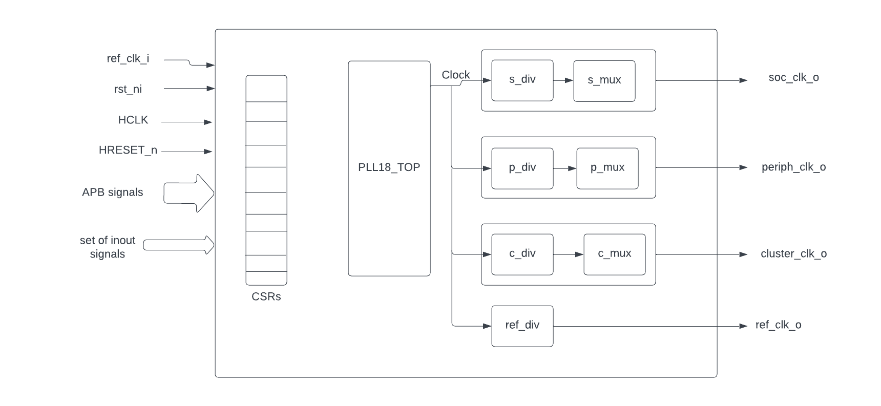
Theory of operaion:-
Inputs:-
ref_clk_i - Reference clock input
rst_ni - To reset the clock divisors and demultiplexers
HCLK -clock for the read and write on the registers
HRESETn - To reset the registers
APB bus signals -Set of APB bus signals
Outputs:-
soc_clk_o - clock for the core soc domain
periph_clk_o - clock for the peripheral domain
cluster_clk_o - clock for the cluster/FPGA domain
ref_clk_o - reference clock which is taken as input
Inouts:-
AVDD, AVDD2,AVSS,VDDC,VSSC
- There are a set of 9 32 bit registers used to control the PLL and
clock divisors.
- When HRESETn is low,all the registers are reset to default values
where control register value is 32’h03000103 and divisor register value is 32’h00A00004,remaining registers are assigned 0.
READ/WRITE into the register:-
- The PLL IP will be in IDLE mode generally.To write or read into the
registers ,first PSEL and PENABLE should be made high.So at every positive clock edge of HCLK,if both PSEL and PENABLE are high then based on whether PWRITE is low or high, PLL IP is changed to READ or WRITE mode so that in next clock cycle read or write operation happen based on the mode and the PLL mode is changed to default IDLE mode after the end of the operation.
Supply of the reference clock to the divisors:-
- Here if RESET register is high or HRESETn pin is low then ,the PLL is
in reset mode(So no outputs are generated).
- If rst_ni is made low,then also there will be no outputs(all the
outputs will be low).
- If the control register BYPASS is high ,then it is in bypass mode
,where the domain clocks of soc,peripherals,and cluster will be the reference clock (ref_clk_i) instead of the divisor clock.
- When BYPASS register is low, the domain clocks are generated from the
reference clock instead of directly passing the reference clock.The generation of domain clocks happen based on the registers value SOC_DIV,PERIPH_DIV,CLUSTER_DIV and REF_DIV .For each divisor the ref clock frequency is reduced by the number of times mentioned in the respective register and that frequency reduced clock is the divisor clock.For example, for soc domain ,the reference clock frequency is reduced by SOC_DIV times and produced clock is the soc domain clock.
How the the transition from divisor clock to ref clock happens when BYPASS is made high
- Whenever the BYPASS is made high from low,then the respective divisor
clock for the domain is stopped as output after completing the next clock cycle and the ref clock starts from there as the domain clock .