APB GPIO
The General Purpose Input/Output (GPIO) IP block supports S/W access to read and write the values on selected I/O, and configuring selected I/O to generate interrupts.
Features
Configurable number of GPIO pins (Upto 128, current implementation supports 32).
Programmable configuration for each pin (output enable, open-drain enable).
Individual control for setting, clearing, or toggling output pins
Pin status reading capability
- Interrupt generation capabilities with multiple configurable types:
Rising edge detection
Falling edge detection
Active low level detection
Active high level detection
Input synchronization to prevent metastability issues.
Block Architecture
The figure below is a high-level block diagram of the APB GPIO module:-
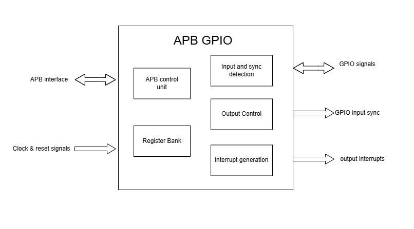
APB GPIO Block Diagram
The APB GPIO IP consists of the following key components:
APB control logic
The APB control logic interfaces with the APB bus to decode and execute commands. It handles CSR reads and writes according to the APB protocol, providing a standardized interface to the system.
GPIO CSR
These CSRs store the configuration for each GPIO pin, including:
Pin configuration (output enable, open-drain enable)
Input value
Output value
Interrupt type configuration
Interrupt enable status
Open-Drain Operation
The GPIO module supports open-drain operation for every GPIO output pin(will depend on the implementation technology). Open-drain is a specific output driver configuration where the GPIO pin can either pull the signal to ground (logic ‘0’) or release it to a high-impedance state, but cannot actively drive it to a high voltage level (logic ‘1’). This configuration requires an external pull-up resistor to achieve a logic ‘1’ state.
The external pull-up resistor must be connected between the GPIO pin and the desired high-voltage level (VDD). Without this pull-up resistor, the pin will remain in an undefined state when not actively driven low.
Input Synchronization
Metastability refers to an unstable state in which the signal fails to settle into a stable low or high level within a required time. A dual-stage synchronizer in the GPIO module prevents metastability issues when sampling external inputs by synchronizing them to the system clock domain. This synchronizer consists of two flip-flops in series, which helps to ensure that any glitches or transient signals on the GPIO inputs are filtered out before being processed by the rest of the system.
The input signals on the GPIO pins are sampled by the first flip-flop, and the output of this flip-flop is then sampled by the second flip-flop. The output of the second flip-flop is the synchronized signal that is used by the GPIO module.
Pin Direction Control
It is assumed, but not required, that each GPIO pin of the CORE-V-MCU is implemented as a bi-directional signal. To enable this, each GPIO signal is associated with three ports of the GPIO module:
gpio_in
gpio_out
gpio_dir
These ports are required to be connected to the appropriate IO PADS provided by the ASIC or FPGA implementation technology. The purpose of the gpio_in and gpio_out ports is self explainatory, and each can be read or written via CSRs (see APB GPIO CSRs below). The function of gpio_dir is determined by the implementation technology. The GPIO module allows gpio_dir to be configured individually for each output pin, via the two-bit DIR field of the SETDIR CSR. Below is a truth table that illustrates how SETDIR allows software to configure the value of gpio_dir.
SETDIR[DIR] |
gpio_dir |
|---|---|
2’b00 |
0 |
2’b01 |
1 |
2’b10 |
!gpio_out |
2’b11 |
!gpio_out |
Typically, gpio_dir is used to drive an active-low output enable of an IO PAD. In such cases, writing SETDIR[DIR][1] to 1’b0 means that software can write SETDIR[DIR][0] to enable or disable the output driver of the IO PAD.
GPIO Input
The GPIO module reads external signals through the gpio_in input signal.
The value of these signals post synchronisation is made available on the PIN0 CSR (address 0x010), allowing the software to read the status of the GPIO input pins.
Each bit in the PIN0 CSR corresponds to a GPIO pin(bit 0 for GPIO pin 0, bit 1 for GPIO pin 1, and so on), where a bit value of 1 indicates a high state and 0 indicates a low state.
The synchronized input signals are also then provided to the gpio_in_sync output signal, which is used by the Advanced Timer module for external event processing.
GPIO Output
The GPIO module drives external devices through the gpio_out output signal.
- The output value of each pin can be controlled by:
OUTx {x = 0 to 3} CSR
SETGPIO, CLRGPIO and TOGGPIO
OUTx CSR is used to drive a group of pins, while SETGPIO, CLRGPIO and TOGGPIO are used to drive a single output pin.
Each bit in the OUT0 CSR corresponds to a GPIO pin(bit 0 for GPIO pin 0, bit 1 for GPIO pin 1, and so on), where a bit value of 1 sets the pin high and a bit value of 0 sets it low.
The SETGPIO CSR (address 0x000) sets a specified pin high.
The CLRGPIO CSR (address 0x004) sets a specified pin low.
The TOGGPIO CSR (address 0x008) toggles the state of a specified pin.
The gpio_out output signal reflects the current output state of the GPIO pins with output enabled via DIR bitfield of SETDIR CSR.
If a output is not enabled for a pin, the corresponding bit in the OUT0 CSR will be 0, as the output value is not applicable for it.
Interrupt Generation
This section describes how GPIO pins generate interrupts and the differences between edge-triggered and level-triggered behavior.
Interrupt Capability
GPIO input pins can be used to receive interrupts from external devices. Since the output value is also reflected on the corresponding input pin, even software can trigger interrupts by driving a particular output pin.
Interrupt Types
The interrupt logic detects events based on the configured type for each of the 32 pins:
Edge-triggered: Detects rising or falling edges
Level-triggered: Detects active-high or active-low levels
The interrupt type for each pin is configured through the SETINT CSR (address 0x03C), which allows the software to specify the desired interrupt behavior.
The interrupt type is specified using bits [19:17]:
000: Active-Low level detection
001: Falling edge detection
010: Rising edge detection
011: Both edges detection
100: Active-High level detection
The interrupt enable status is specified using bit [16]:
0: Disable interrupt for the pin
1: Enable interrupt for the pin
The pin number is specified using bits [6:0], allowing the software to configure interrupts for individual pins.
For example, to configure GPIO input pin 0 for rising edge detection, the software would write the following values to the SETINT CSR:
`
SETINT = (0b010 << 17) | (1 << 16) | (0 << 6)
`
This sets the interrupt type to rising edge detection, enables the interrupt, and selects GPIO pin 0.
Interrupt Signal Behavior
When an event occurs on an input pin configured for interrupts, the interrupt logic asserts the corresponding interrupt signal for that pin. This signal is represented by the interrupt output signal, which is a 32-bit vector where each bit corresponds to a GPIO pin. For example, if GPIO pin 0 is configured for interrupts and an event occurs, the interrupt[0] signal will be asserted (set to high). This signal remains high for one clock cycle to indicate the event, after which it is cleared.
The interrupt signal is captured by the APB Event Controller for further processing. Refer to the APB Event Controller documentation for more details.
Edge vs. Level-Triggered Interrupts
The main difference between edge-triggered and level-triggered interrupts lies in how they are generated and cleared:
Edge-triggered interrupts are activated on signal transitions (rising or falling edges) and are automatically cleared after one clock cycle.
Level-triggered interrupts remain active as long as the level condition (high or low) persists, to resolve this the GPIO module blocks the level-triggered interrupt signal after it is generated once and deasserts the output interrupt.
Hence, both edge-triggered and level-triggered interrupts are asserted for one clock cycle, but level-triggered interrupts require explicit acknowledgment to allow new interrupts to be generated.
Interrupt Acknowledgment
To prevent repeated triggering from persistent level conditions, the APB GPIO disables the interrupt signal after it is generated once and deasserts the output interrupt. The APB master must acknowledge the interrupt by writing to the INTACK CSR.
Once acknowledged, the GPIO can reassert the interrupt signal if the level condition still holds true. The above is only valid for level-triggered interrupts, as edge-triggered interrupts are automatically cleared after one clock cycle.
System Architecture
The figure below depicts the connections between the GPIO and rest of the modules in CORE-V-MCU:-
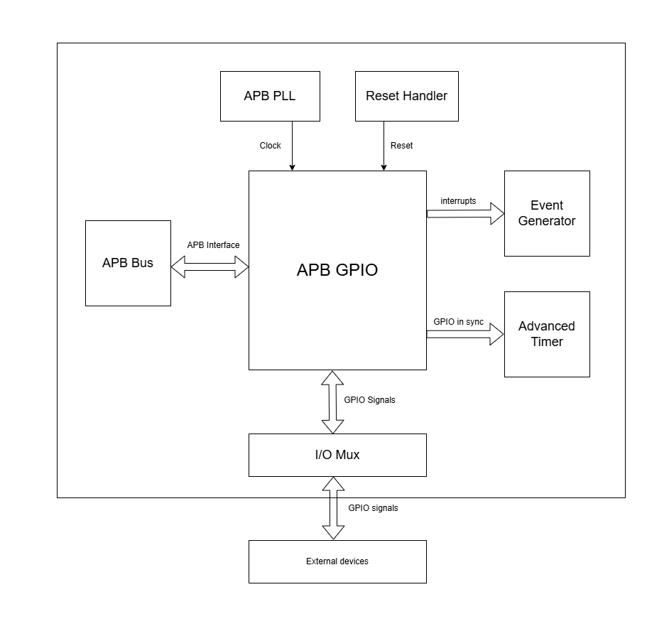
APB GPIO CORE-V-MCU connections diagram
The gpio_in_sync output is directly connected to the Advanced Timer module. It provides synchronized GPIO input signals that serve as external event sources for the Advanced Timer. These signals are processed by the Advanced Timer logic and can ultimately control the up/down counter functionality. This integration enables external events captured by GPIO pins to influence timer operations.
Programming View Model
The APB GPIO IP follows a simple programming model:
GPIO Pin Configuration
- Each GPIO pin can be configured individually:
Configure the pin direction/configuration (output enable, open-drain) using the SETDIR CSR
Configure interrupt behavior if necessary using the SETINT CSR
For details, please refer to the ‘Firmware Guidelines’.
GPIO Pin Control
- To control GPIO pins:
Use SETGPIO to set a pin high
Use CLRGPIO to set a pin low
Use TOGGPIO to toggle a pin’s state
Use OUTx CSRs to set multiple pins at once
For details, please refer to the ‘Firmware Guidelines’.
GPIO Pin Status
- To read GPIO pin status:
Use RDSTAT to read a selected pin’s status
Use PINx CSRs to read the status of multiple pins at once
For details, please refer to the ‘Firmware Guidelines’.
Interrupt Handling
- When an interrupt occurs:
Determine the source by reading pin status
Handle the interrupt according to application requirements
Acknowledge the interrupt using the INTACK CSR in case of level-triggered interrupts.
For details, please refer to the ‘Firmware Guidelines’.
APB GPIO CSRs
The APB GPIO has a 4KB address space and the CSR interface designed using the APB protocol. There are multiple CSRs allowing the processor to read input GPIO pin states, set output pin values, and configure various GPIO settings such as interrupt behavior, pin direction etc. The CSRs are designed for 128 GPIO pins, but the current implementation supports only 32 GPIO pins.
NOTE: Several of the Event Controller CSR are volatile, meaning that their read value may be changed by the hardware. For example, the value of PIN0 CSR may change if the GPIO pin is configured as an input and the external signal changes. However, the non-volatile CSRs, as the name suggests, will retain their value until explicitly changed by the software.
SETGPIO
Address Offset: 0x000
Type: non-volatile
Field |
Bits |
Access |
Default |
Description |
|---|---|---|---|---|
PIN_SELECT |
[6:0] |
WO |
0x0 |
GPIO pin index, which will be set high Only pins with output enabled can be set high |
CLRGPIO
Address Offset: 0x004
Type: non-volatile
Field |
Bits |
Access |
Default |
Description |
|---|---|---|---|---|
PIN_SELECT |
[6:0] |
WO |
0x0 |
GPIO pin index, which will be set low Only pins with output enabled can be set low |
TOGGPIO
Address Offset: 0x008
Type: non-volatile
Field |
Bits |
Access |
Default |
Description |
|---|---|---|---|---|
PIN_SELECT |
[6:0] |
WO |
0x0 |
GPIO pin index, which will be toggled Only pins with output enabled can be toggled |
PIN0
Address Offset: 0x010
Type: volatile
Field |
Bits |
Access |
Default |
Description |
|---|---|---|---|---|
GPIO_IN |
[31:0] |
RO |
0x0 |
Read status of GPIO pins 31:0 |
PIN1
Address Offset: 0x014
Type: volatile
Field |
Bits |
Access |
Default |
Description |
|---|---|---|---|---|
GPIO_IN |
[31:0] |
RO |
0x0 |
Read status of GPIO pins 63:32 (Not supported) |
PIN2
Address Offset: 0x018
Type: volatile
Field |
Bits |
Access |
Default |
Description |
|---|---|---|---|---|
GPIO_IN |
[31:0] |
RO |
0x0 |
Read status of GPIO pins 95:64 (Not supported) |
PIN3
Address Offset: 0x01C
Type: volatile
Field |
Bits |
Access |
Default |
Description |
|---|---|---|---|---|
GPIO_IN |
[31:0] |
RO |
0x0 |
Read status of GPIO pins 127:96 (Not supported) |
OUT0
Address Offset: 0x020
Type: volatile
Field |
Bits |
Access |
Default |
Description |
|---|---|---|---|---|
GPIO_OUT |
[31:0] |
RW |
0x0 |
Set value of GPIO pins 31:0. If output is enabled for the pin |
OUT1
Address Offset: 0x024
Type: volatile
Field |
Bits |
Access |
Default |
Description |
|---|---|---|---|---|
GPIO_OUT |
[31:0] |
RW |
0x0 |
Set value of GPIO pins 63:32. If output is enabled for the pin. (Not supported) |
OUT2
Address Offset: 0x028
Type: volatile
Field |
Bits |
Access |
Default |
Description |
|---|---|---|---|---|
GPIO_OUT |
[31:0] |
RW |
0x0 |
Set value of GPIO pins 95:64. If output is enabled for the pin. (Not supported) |
OUT3
Address Offset: 0x02C
Field |
Bits |
Access |
Default |
Description |
|---|---|---|---|---|
GPIO_OUT |
[31:0] |
RW |
0x0 |
Set value of GPIO pins 127:96. If output is enabled for the pin. (Not supported) |
SETSEL
Address Offset: 0x030
Type: non-volatile
Field |
Bits |
Access |
Default |
Description |
|---|---|---|---|---|
PIN_SELECT |
[6:0] |
WO |
0x0 |
GPIO pin number to select for reading pin using RDSTAT |
RDSTAT
Address Offset: 0x034
Type: volatile
Field |
Bits |
Access |
Default |
Description |
|---|---|---|---|---|
DIR |
[25:24] |
RO |
0x0 |
Direction configuration for pin selected via SETSEL CSR or last selected pin. |
INT_TYPE |
[19:17] |
RO |
0x0 |
Interrupt type configuration for pin selected via SETSEL CSR or last selected pin. |
INT_EN |
[16] |
RO |
0x0 |
Interrupt enable status for pin selected via SETSEL CSR or last selected pin. |
PIN_IN |
[12] |
RO |
0x0 |
Input value of pin selected via SETSEL CSR or last selected pin. |
PIN_OUT |
[8] |
RO |
0x0 |
Output value of pin selected via SETSEL CSR or last selected pin. Only valid when DIR value is 01 |
PIN_SELECT |
[6:0] |
RO |
0x0 |
Currently selected pin number selected via SETSEL CSR or last selected pin. |
SETDIR
Address Offset: 0x038
Type: non-volatile
Field |
Bits |
Access |
Default |
Description |
|---|---|---|---|---|
DIR |
[25:24] |
WO |
0x0 |
Direction Configuration:
|
PIN_SELECT |
[6:0] |
WO |
0x0 |
GPIO pin number to configure |
SETINT
Address Offset: 0x03C
Type: non-volatile
Field |
Bits |
Access |
Default |
Description |
|---|---|---|---|---|
INT_TYPE |
[19:17] |
WO |
0x0 |
Interrupt type: 000: Active-Low level 001: Falling edge 010: Rising edge 011: Both edges 100: Active-High level |
INT_EN |
[16] |
WO |
0x0 |
Interrupt enable: 0: Disable 1: Enable |
PIN_SELECT |
[6:0] |
WO |
0x0 |
GPIO pin number to configure interrupt |
INTACK
Address Offset: 0x040
Type: non-volatile
Field |
Bits |
Access |
Default |
Description |
|---|---|---|---|---|
PIN_NUM |
[7:0] |
WO |
0x0 |
GPIO pin number to acknowledge interrupt |
Firmware Guidelines
GPIO Pin Configuration Procedure
Configuring Pin Direction
- Direction of a pin can be configured by writing to the SETDIR CSR (address 0x038).
To configure gpio_in as input: All pins are input by default and the input cannot be disabled.
To configure gpio_out as output: Place a value of 1 in bit [24] along with the pin number in bits [6:0].
To configure gpio_out as open-drain: Place a value of 1 in bit [25] along with the pin number in bits [6:0].
Configuring Interrupt Behavior
If the input pin requires interrupt capability, write to the SETINT CSR (address 0x03C).
Include the pin number in bits [6:0].
To enable interrupts, set bit [16] to 1; to disable, set to 0.
- To configure interrupt type, set bits [19:17] as follows:
000: Active-Low level detection
001: Falling edge detection
010: Rising edge detection
011: Both edges detection
100: Active-High level detection
If output is enabled for a pin and interrupt is also configured, then driving the pin through software will also result in interrupt generation.
GPIO Status Reading Procedure
Reading Individual Pin Status
First, select the desired pin by writing its number to SETSEL CSR(address 0x030).
Read the RDSTAT CSR (address 0x034).
Examine bit [12] for the current input state of the pin.
Examine bit [8] for the current output value.
- Other fields provide configuration information:
Bits [25:24]: Direction configuration(output enabled, open-drain enabled)
Bits [19:17]: Interrupt type(active-low, falling edge, rising edge, both edges, or active-high)
Bit [16]: Interrupt enable status
Reading Multiple Pin States
To read the status of multiple pins at once, read the PIN0 CSR, in which each bit represents corresponding output pin.
A bit value of 1 indicates a high state, 0 indicates a low state.
GPIO Control Procedure
Setting Individual Pins High
Write the pin number to the SETGPIO CSR (address 0x000).
This operation sets the specified pin to a high state.
Setting Individual Pins Low
Write the pin number to the CLRGPIO CSR (address 0x004).
This operation sets the specified pin to a low state.
Toggling Individual Pins
Write the pin number to the TOGGPIO CSR (address 0x008).
This inverts the current state of the specified pin.
Controlling Multiple Pins Simultaneously
To control multiple pins in one operation, write to the OUT0 CSR.
Each bit position corresponds to the respective pin number.
Setting a bit to 1 drives the corresponding pin high; setting to 0 drives it low.
Interrupt Handling Procedure
Interrupt Processing
When an interrupt occurs, the GPIO module asserts the corresponding interrupt signal.
Process the interrupt according to application requirements.
For level-sensitive interrupts, the interrupt needs to be acknowledged/unblocked before it can be reasserted.
Interrupt Acknowledgment
To acknowledge the interrupt, write the pin number to the INTACK CSR (address 0x040).
This clears the interrupt signal for the specified pin, allowing it to be reasserted if the condition persists.
Note that this acknowledgment is only required for level-triggered interrupts.
Open-Drain Configuration Guidelines
Configuring Open-Drain Mode
Write to SETDIR with a value of 1 in bit [25] enabling open drain configuration.
Include the pin number in bits [6:0].
Using Open-Drain Pins
To drive the pin low: Use SETGPIO or write a 1 to the corresponding bit in OUT0.
To place the pin in high-impedance state: Use CLRGPIO or write a 0 to the corresponding bit in OUT0.
Ensure an external pull-up resistor is connected to the pin to achieve a high state when not driven low.
Pin Diagram
The figure below represents the input and output pins for the APB GPIO:-
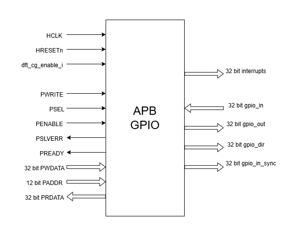
APB GPIO Pin Diagram
Clock and Reset
HCLK: System clock input; provided by APB FLL.
HRESETn: Active-low reset signal for initializing all internal CSRs and logic.
dft_cg_enable_i: Clock gating enable input for DFT or low-power scenarios; Always 0 in the current implementation.
APB Interface Signals
PADDR[11:0]: APB address bus input
PWDATA[31:0]: APB write data bus input
PWRITE: APB write control input (high for write, low for read)
PSEL: APB peripheral select input
PENABLE: APB enable input
PRDATA: APB write data bus input
PREADY: APB ready output to indicate transfer completion
PSLVERR: APB error response output signal
GPIO Data Signals
gpio_in[31:0]: External GPIO input values from the physical pins; provided by external devices.
gpio_in_sync[31:0]: Synchronized version of gpio_in, provides the external signals to Advanced timer block.
gpio_out[31:0]: Output values driven onto physical GPIO pins, if pin is configured as outputs; provided to external devices.
gpio_dir[31:0]: Direction control per pin; provided to external devices.
Interrupt Signals
interrupt[31:0]: Per-pin interrupt outputs, asserted based on edge or level-triggered conditions; provided to APB Event Controller.