APB SoC controller
This APB peripheral primarily controls I/O configuration and serves as the central configuration hub in the CORE-V-MCU for pad multiplexing, boot control, watchdog monitoring, and eFPGA interfacing.
Features
Control interface for configurable pad multiplexer and IO configuration
Watchdog timer with programmable timeout and reset capability
JTAG CSR access for debug and configuration
Boot address and fetch enable control for the Fabric Controller (FC)
eFPGA control and configuration interface
Ready timeout monitoring for system-level recovery
System information and status CSRs
Soft reset capability for all APB Client Peripherals
Build date and time information
Block Architecture
The figure below is a high-level block diagram of the APB SoC Controller module:-
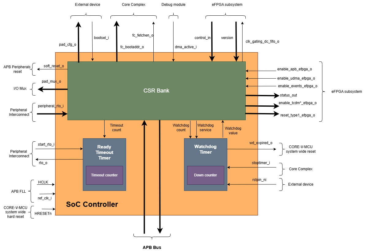
APB SoC Controller Block Diagram
The APB SoC Controller IP consists of the following key components:
Pad Configuration
The controller manages pad multiplexing and configuration for all system IOs. It provides the multiplexing information to the Pad control module, which directly manages the IO pads.
Each pad can be individually configured for:
Pad multiplexing (selecting the pad function, i.e. connecting the I/O to different signals in CORE-V-MCU)
Pad electrical configuration (drive strength, pull-up/down, etc. These configurations are not implemented in the current design.)
- These configurations can be accessed through two methods, which can be used as per user preference:
- Directly through the IO_CTRL CSRs (0x400 - 0x4C0)
Individual CSR for each pad, allowing direct access to the pad configuration.
- Each CSR is 32 bits wide, with the following fields:
PADMUX specifies the pad multiplexing configuration
PADCFG specifies the electrical configuration of the pad(TBD)
- Through the WCFGFUN and RCFGFUN CSRs (0x60 and 0x64).
- WCFGFUN CSR is used to configure the pad multiplexing and electrical configuration.
The IO_PAD field in WCFGFUN CSR specifies the pad index to be configured.
The PADMUX field in WCFGFUN CSR specifies the pad multiplexing configuration.
The PADCFG field in WCFGFUN CSR specifies the electrical configuration of the pad(TBD).
- RCFGFUN CSR is used to read the current configuration of a specific pad.
The IO_PAD field in RCFGFUN CSR specifies the pad index to be read.
The PADMUX field in RCFGFUN CSR specifies the current pad multiplexing configuration.
The PADCFG field in RCFGFUN CSR specifies the current electrical configuration of the pad(TBD).
To use RCFGFUN CSR, the IO_PAD field must be set to the pad index of interest, and then a read operation is performed.
The read operation will return the current configuration of the specified pad.
An example of using the WCFGFUN and RCFGFUN CSRs for pad multiplexing is as follows:
If you want to configure the pad with index 12, there are 4 possible configurations for the pad multiplexing, i.e. 00, 01, 10, and 11.
- In the case of pad with index 12, the 4 multiplexing configurations are:
00: GPIO pin 0
01: UART 1 RX pin
10: GPIO pin 5
11: eFPGA IO pin 5
Let’s suppose you want to configure the pad with index 12 to be used as UART 1 RX pin.
- You can do this by writing the following value to the WCFGFUN CSR:
- WCFGFUN = 0x00000001
PADMUX = 0x01 (UART 1 RX pin)
IO_PAD = 0x0C (pad index 12)
PADCFG = 0x01 (electrical configuration, which is not implemented in the current design)
- After writing the WCFGFUN CSR, you can read the RCFGFUN CSR to verify the configuration:
First you will have to set the IO_PAD field in RCFGFUN CSR to 0x0C (pad index 12).
- Then you can read the RCFGFUN CSR, which will return the following value:
- RCFGFUN = 0x00000001
PADMUX = 0x01 (UART 1 RX pin)
IO_PAD = 0x0C (pad index 12)
PADCFG = 0x01 (electrical configuration, which is not implemented in the current design)
Note: Pad multiplexing details can be found in the IO Assignment document.
Watchdog Timer
A programmable watchdog timer(WDT) runs on the reference clock(ref_clk_i) and resets the system when expired. The watchdog timer is a safety feature designed to detect and recover from system malfunctions.
Initialization and Configuration
On system power-up, the watchdog timer is disabled by default.
- The timeout period of the watchdog timer can be configured using the WD_COUNT CSR. The default value of WD_COUNT is 0x8000
Note: WD_COUNT is only writable when the watchdog is disabled.
The watchdog is enabled by setting the ENABLE_STATUS (bit 31) in the WD_CONTROL CSR.
After enabling, the watchdog timer begins counting down from the value set in the WD_COUNT CSR and decrements on each positive edge of the reference clock (ref_clk_i), given that the stoptimer_i signal is not asserted.
If the stoptimer_i signal is asserted, the watchdog timer will be paused and will not decrement until the stoptimer_i signal is deasserted.
The stoptimer_i is asserted by the Core-Complex when the Core is in debug mode.
Expiration
The watchdog timer is considered expired when the counter reaches one.
- When the watchdog timer expires, the following occurs:
The wd_expired_o signal is asserted for one clock cycle to indicate the expiration.
The reset reason is set to 2’b11 in the RESET_REASON CSR, indicating a watchdog expiration.
A system-wide reset is triggered.
The system-wide reset is received in the SoC Controller as well through the HRESETn signal.
This resets all the CSRs and output pins(including wd_expired_o) in the SoC Controller, including the WD_CONTROL and WD_COUNT CSRs, thereby disabling the watchdog timer and setting the WD_COUNT CSR to its default value of 0x8000.
Servicing the Watchdog
Periodically resetting the watchdog timer is essential to prevent it from expiring, this is known as servicing the watchdog.
To prevent expiration(servicing the watchdog timer), software must periodically write the magic value 0x6699 to the WD_CONTROL CSR.
The watchdog can also be serviced by setting the ENABLE_STATUS bit in the WD_CONTROL CSR.
Servicing resets the counter to the value configured in WD_COUNT CSR and the watchdog timer continues counting down from that value.
Resetting Watchdog Timer
Once the watchdog timer is enabled, it can be reset or updated only if the watchdog reset request is received, i.e. rstpin_ni is asserted and deasserted.
If a reset request is initiated via the rstpin_ni pin, then the watchdog timer is set to its default value of 0x8000.
The reset reason is recorded in the RESET_REASON CSR with the value 1.
The watchdog timer will not start counting down until the rstpin_ni signal is deasserted.
Disabling the Watchdog Timer
Once enabled, the watchdog timer cannot be disabled. However, it can be effectively disabled by performing a system reset, i.e. asserting the HRESETn signal.
Stopping the Watchdog Timer
- The watchdog timer can be stopped when the stoptimer_i signal is asserted.
The stoptimer_i is asserted by the Core-Complex when the Core is in debug mode.
When the stoptimer_i signal is asserted, the watchdog timer stops counting down and holds its current value.
The watchdog timer resumes counting down from the held value when the stoptimer_i signal is deasserted.
This allows to stop the watchdog timer temporarily without resetting it.
eFPGA Interface
The SoC Controller provides comprehensive management of the embedded FPGA (eFPGA) interface, enabling configuration, control, and monitoring of the eFPGA subsystem. Key features:
Reset control for the eFPGA quadrants (left bottom, right bottom, right top, left top)
Interface enabling/disabling for various eFPGA connections (TCDM, APB, events)
Status monitoring and CSR access for eFPGA operations
Version information access for the eFPGA subsystem
Initialization and Configuration
On system reset, all eFPGA interfaces are disabled by default and have to be explicitly enabled.
Interfaces are enabled via the ENABLE_IN_OUT_EFPGA CSR and are communicated through various enable signals to the eFPGA.
Reset control is asserted and deasserted through the RESET_TYPE1_EFPGA CSR, which allows resetting of individual eFPGA quadrants and is communicated through the 4-bit reset_type1_efpga_o signal.
Additional features are controlled through the EFPGA_CONTROL CSR and the same is communicated through the 32-bit control_in signal.
Monitoring
The EFPGA_STATUS CSR provides visibility into the operational state of the eFPGA. The 32-bit status signals(status_out) from eFPGA are made available on this CSR to make them accessible through the APB interface.
The EFPGA_VERSION CSR allows software to determine the eFPGA IP version. The 8-bit version signals(version) from eFPGA are made available on this CSR to make them accessible through the APB interface.
Power Management
- Clock gating can be selectively applied to eFPGA-related FIFOs and is provided through the clk_gating_dc_fifo_o signal to eFPGA.
Note: As per current design, clk_gating_dc_fifo_o is always set to 1.
Ready Timeout Mechanism
The Ready Timeout (RTO) mechanism is a system protection feature that monitors bus transaction timeouts. The SoC Controller generates a timeout signal (rto_o) when a peripheral fails to respond within the specified time limit. It improves system robustness by preventing the bus from stalling indefinitely due to unresponsive peripherals.
The RTO mechanism is segregated into two IPs, the SoC Controller and the SoC Peripheral Interconnect.
Operation
When a bus transaction starts, the SoC peripheral interconnect asserts the start_rto_i pin on the SoC Controller.
The SoC Controller, when its start_rto_i pin is asserted, starts counting down from the value set in the RTO_COUNT CSR and decrements on each positive edge of the system clock (HCLK).
The counter starts counting down from the value set in the RTO_COUNT CSR and decrements on each positive edge of the system clock(HCLK).
The RTO_COUNT CSR of the SoC controller defines the timeout threshold.
If the SoC Peripheral Interconnect deasserts the start_rto_i signal before the SOC controller timeout counter reaches zero, then the counter is reloaded, and no timeout is signalled.
If the SOC Peripheral Interconnect fails to respond by deasserting the start_rto_i signal before the SOC controller timeout counter reaches zero, then the SOC controller asserts an rto_o signal to the SOC Peripheral Interconnect to indicate a timeout.
The SOC Peripheral Interconnect, when its rto_i is asserted, drives the peripheral_rto_i pin of the SOC Peripheral Interconnect to indicate which peripheral caused the timeout.
The SOC peripheral controller captures the faulty peripheral information in RTO_PERIPHERAL CSR to indicate which core-v-mcu peripheral caused the timeout.
The RTO_PERIPHERAL CSR consists of 9 bits, each bit representing a specific peripheral. When the peripheral_rto_i pin is updated, the values of the corresponding bits in the RTO_PERIPHERAL CSR are set to 1.
In the next clock cycle, the SoC controller deasserts the rto_o signal.
The SoC Peripheral Interconnect, when its rto_i is deasserted, clears the peripheral_rto_i pin.
The RTO_PERIPHERAL CSR is clear-on-write, i.e. writing to this CSR will clear it, and the write value is ignored.
Boot Control
The boot control mechanism manages the system boot process, determining the behaviour of the Fabric Controller/Core-Complex during reset and initial execution. It allows flexible configuration of boot address, fetch control, and boot mode selection. This mechanism enables software and hardware to coordinate system boot through configurable registers and external signals, supporting multiple boot modes and sources.
Boot Address Configuration
On system reset, the default boot address is set to 0x1A000080.
The boot address can be modified by writing a new value to the FCBOOT CSR.
Fetch Control
- The Fabric Controller/Core-Complex’s activity is gated by the fc_fetchen_o signal, i.e. allowing dynamic enable/disable of instruction fetch.
The default value of fc_fetchen_o is ,1 i.e instruction fetch is enabled.
This signal is controlled through the FCFETCH CSR.
Boot Mode Selection
- Boot mode defines how and from where a system loads the code needed to start operating.
- Boot mode is influenced by external hardware signals:
- bootsel_i: Selects between different boot paths.
1 = SPI boot
0 = Host mode via I2Cs
dmactive_i: Indicates debug mode active status.
The selected boot mode and current boot status, as well as the debug mode status, are captured in the BOOTSEL CSR.
JTAG Interface
The SoC Controller provides an interface to the JTAG debug port, enabling bidirectional communication and control for system-level debugging. Key features:
Bidirectional communication through 8-bit-wide JTAG_REG_IN and JTAG_REG_OUT bitfields of JTAGREG CSR
External JTAG signals are synchronised to the internal system clock (HCLK) to ensure reliable data exchange.
Data Access and Communication
The upper bits of JTAGREG are updated with incoming JTAG data from an external device through the soc_jtag_reg_i port.
The lower bits of JTAGREG can be written by software to transmit data to the external JTAG device through the soc_jtag_reg_i port.
This bidirectional access enables debug communication, such as status reporting, control signalling, or debug-triggered behaviours.
Soft Reset Mechanism
The soft reset mechanism allows the SoC Controller to reset all APB client peripherals connected to the APB bus without requiring a full system reset. This feature is useful for recovering from peripheral malfunctions or reinitialising peripherals during runtime.
Operation
Writing any value to the SOFT_RESET CSR (at offset 0x00FC) initiates the soft reset sequence.
The write value is ignored, as the CSR acts as a write-only strobe.
Upon triggering, the soft_reset_o signal is asserted, propagating the reset to all APB client peripherals.
- APB client peripheral includes the following:
I2C Slave
Event Controller
Advanced Timer
GPIO
Timer
FLL
uDMA subsystem
eFPGA subsystem
The SoC Controller itself is only partially reset, retaining WDT and Boot Control configurations.
- The following CSRs in the SoC Controller are reset to their default values:
WCFGFUN
RCFGFUN
IO_CTRL (0x400-0x4C0)
RESET_TYPE1_EFPGA
ENABLE_IN_OUT_EFPGA
EFPGA_CONTROL_IN
RTO_PERIPHERAL
READY_TIMEOUT_COUNT
- The following output pins, which are controlled through the CSRs, are reset to reflect their default values:
pad_mux_o
pad_cfg_o
reset_type1_efpga_o
clk_gating_dc_fifo_o
enable_udma_efpga_o
enable_events_efpga_o
enable_apb_efpga_o
enable_tcdm3_efpga_o
enable_tcdm2_efpga_o
enable_tcdm1_efpga_o
enable_tcdm0_efpga_o
control_in
- The reset signal(soft_reset_o) is deasserted when:
The system reset is issued due to the HRESETn signal being asserted.
The pos-edge of the HCLK signal is encountered.
System Architecture
The figure below depicts the connections between the SoC Controller and the rest of the modules in CORE-V-MCU:-
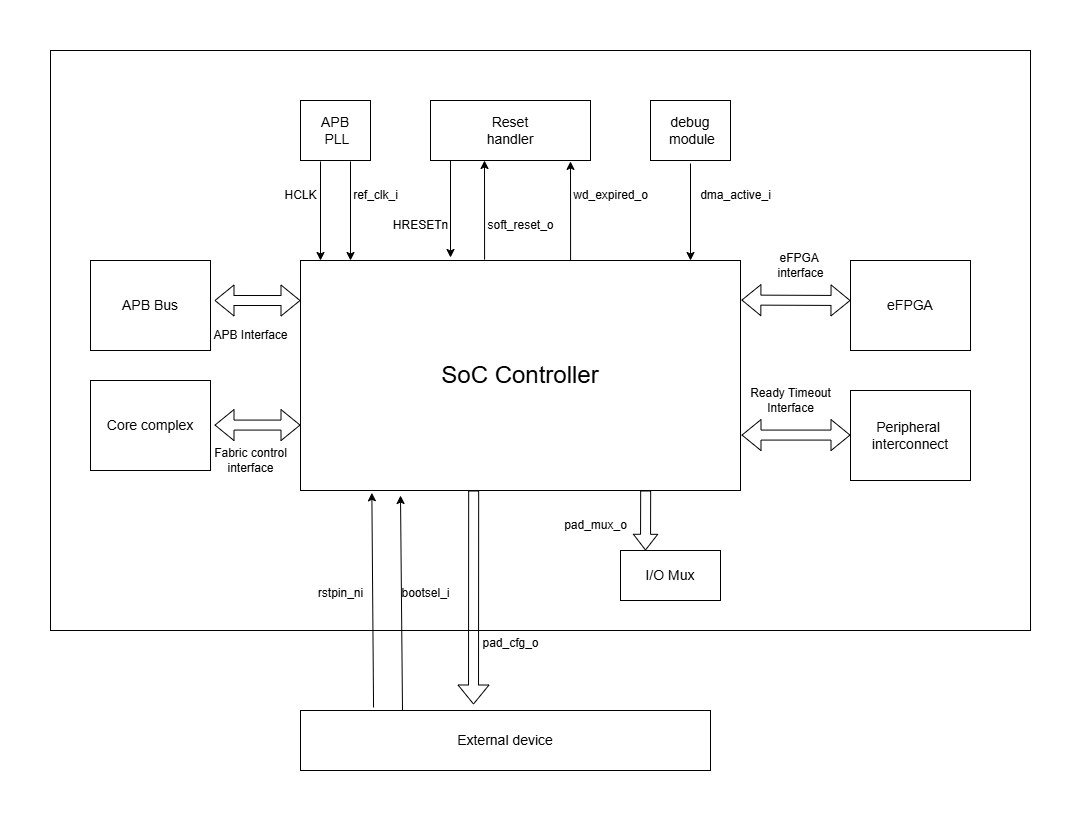
APB SoC Controller CORE-V-MCU connections diagram
Programming View Model
The APB SOC Controller is memory-mapped at a base address defined by the system. All CSRs are accessible via standard APB read/write operations.
CSR Access
- CSRs are accessed using 32-bit reads and writes over the APB bus. The address space is organised as follows:
Base CSRs: 0x000 - 0x0FC
Pad configuration CSRs: 0x400 - 0x4C0
Programming Sequence
- Typical programming sequences include:
Read system information from INFO CSR
Configure boot address and fetch enable
Set up pad configuration and multiplexing
Configure watchdog timer if needed
Set up eFPGA control parameters
Monitor status CSRs as needed
APB SoC Controller CSRs
Refer to Memory Map for the peripheral domain address of the SoC Controller.
NOTE: Several of the SoC Controller CSR are volatile, meaning that their read value may be changed by the hardware. For example, writing the RCFGFUN CSR will set the I/O port to be read. A subsequent read will return the configuration of the I/O port. As the name suggests, the value of non-volatile CSRs is not changed by the hardware. These CSRs retain the last value written by the software. A CSR’s volatility is indicated by its “type”.
Details of CSR access type are explained here.
INFO
Address Offset = 0x0000
Type: non-volatile
Field |
Bits |
Access |
Default |
Description |
|---|---|---|---|---|
N_CORES |
31:16 |
RO |
0x1 |
Number of cores in design |
N_CLUSTERS |
15:0 |
RO |
0x0 |
Number of clusters in design |
FCBOOT
Address Offset = 0x0004
Type: non-volatile
Field |
Bits |
Access |
Default |
Description |
|---|---|---|---|---|
BOOT_ADDR |
31:0 |
RW |
0x1A000080 |
Boot address for the FC core |
FCFETCH
Address Offset = 0x0008
Type: non-volatile
Field |
Bits |
Access |
Default |
Description |
|---|---|---|---|---|
ENABLE |
0:0 |
RW |
0x1 |
Fetch enable bit Signals FC to initiate instruction fetching and processing |
BUILD_DATE
Address Offset = 0x000C
Type: non-volatile
Field |
Bits |
Access |
Default |
Description |
|---|---|---|---|---|
YEAR |
31:16 |
RO |
0x0 |
Year in binary-coded decimal format |
MONTH |
15:8 |
RO |
0x0 |
Month in binary-coded decimal format |
DAY |
7:0 |
RO |
0x0 |
Day in binary-coded decimal format |
BUILD_TIME
Address Offset = 0x0010
Type: non-volatile
Field |
Bits |
Access |
Default |
Description |
|---|---|---|---|---|
HOUR |
23:16 |
RO |
0x0 |
Hour in binary-coded decimal format |
MINUTES |
15:8 |
RO |
0x0 |
Minutes in binary-coded decimal format |
SECONDS |
7:0 |
RO |
0x0 |
Seconds in binary-coded decimal format |
WCFGFUN
Address Offset = 0x0060
type: non-volatile
Field |
Bits |
Access |
Default |
Description |
|---|---|---|---|---|
RESERVED |
31:30 |
RO |
0x0 |
Reserved |
PADCFG |
29:24 |
RW |
0x1 |
|
RESERVED |
23:18 |
RO |
0x0 |
Reserved |
PADMUX |
17:16 |
RW |
0x0 |
Pad mux configuration |
RESERVED |
15:6 |
RO |
0x0 |
Reserved |
IO_PAD |
5:0 |
RW |
0x0 |
IO pad index to be configured |
RCFGFUN
Address Offset = 0x0064
type: volatile
Field |
Bits |
Access |
Default |
Description |
|---|---|---|---|---|
RESERVED |
31:30 |
RO |
0x0 |
Reserved |
PADCFG |
29:24 |
RO |
0x1 |
|
RESERVED |
23:18 |
RO |
0x0 |
Reserved |
PADMUX |
17:16 |
RO |
0x0 |
Pad mux configuration |
RESERVED |
15:6 |
RO |
0x0 |
Reserved |
IO_PAD |
5:0 |
RW |
0x0 |
IO pad index to be read |
JTAGREG
Address Offset = 0x0074
Type: volatile
Field |
Bits |
Access |
Default |
Description |
|---|---|---|---|---|
RESERVED |
31:16 |
RO |
0x0 |
Reserved |
JTAG_REG_IN |
15:8 |
RO |
0x0 |
shows the data present at soc_jtag_reg_i port |
JTAG_REG_OUT |
7:0 |
RW |
0x0 |
data to be driven on soc_jtag_reg_o port |
BOOTSEL
Address Offset = 0x00C4
Type: volatile
Field |
Bits |
Access |
Default |
Description |
|---|---|---|---|---|
BOOTSEL |
0:0 |
RO |
Configured from bootsel_i pin on reset |
|
DMACTIVE |
1:1 |
RO |
0x0 |
DMA active value configured from dmactive_i pin on reset |
RESERVED |
29:2 |
RO |
0x0 |
Reserved |
BOOTSEL_IN |
30 |
RO |
Current status of bootsel_i pin |
|
DMACTIVE_IN |
31 |
RO |
0x0 |
Current status of dmactive_i pin |
CLKSEL
Address Offset = 0x00C8
Type: volatile
Field |
Bits |
Access |
Default |
Description |
|---|---|---|---|---|
SELECT |
0:0 |
RO |
0x1 |
Shows current status of sel_fll_clk_i pin |
WD_COUNT
Address Offset = 0x00D0
Type: volatile
Field |
Bits |
Access |
Default |
Description |
|---|---|---|---|---|
COUNT |
30:0 |
RW |
0x8000 |
Watchdog timer initial value Only writable when Watchdog is disabled |
WD_CONTROL
Address Offset = 0x00D4
Type: volatile
Field |
Bits |
Access |
Default |
Description |
|---|---|---|---|---|
ENABLE_STATUS |
31:31 |
RW |
0x0 |
1=Watchdog Enabled, 0=Watchdog not enabled. Note: Once enabled, can only be disabled through asserting HRESETn i.e. resetting the whole SoC Controller |
WD_VALUE |
15:0 |
RW |
0x8000 |
Read & write to this bitfield access different information. Read: Current value of watchdog timer Write: Write to this bitfield are not captured. If the value is 0x6699, then the watchdog timer is reset. Any other value does not have any impact. |
RESET_REASON
Address Offset = 0x00D8
Type: volatile
Field |
Bits |
Access |
Default |
Description |
|---|---|---|---|---|
REASON |
1:0 |
RC |
0x0 |
2’b01= reset pin(rstpin_ni) asserted 2’b11=Watchdog expired |
RTO_PERIPHERAL
Address Offset = 0x00E0
Type: volatile
Configured from peripheral_rto_i pin
Field |
Bits |
Access |
Default |
Description |
|---|---|---|---|---|
FCB_RTO |
8:8 |
RWC |
0x0 |
1 indicates that the FCB interface caused a ready timeout |
TIMER_RTO |
7:7 |
RWC |
0x0 |
1 indicates that the TIMER interface caused a ready timeout |
I2CS_RTO |
6:6 |
RWC |
0x0 |
1 indicates that the I2CS interface caused a ready timeout |
EVENT_GEN_RTO |
5:5 |
RWC |
0x0 |
1 indicates that the EVENT GENERATOR interface caused a ready timeout |
ADV_TIMER_RTO |
4:4 |
RWC |
0x0 |
1 indicates that the ADVANCED TIMER interface caused a ready timeout |
SOC_CONTROL_R TO |
3:3 |
RWC |
0x0 |
1 indicates that the SOC CONTROL interface caused a ready timeout |
UDMA_RTO |
2:2 |
RWC |
0x0 |
1 indicates that the UDMA CONTROL interface caused a ready timeout |
GPIO_RTO |
1:1 |
RWC |
0x0 |
1 indicates that the GPIO interface caused a ready timeout |
FLL_RTO |
0:0 |
RWC |
0x0 |
1 indicates that the FLL interface caused a ready timeout |
READY_TIMEOUT_COUNT
Address Offset = 0x00E4
Type: volatile
Field |
Bits |
Access |
Default |
Description |
|---|---|---|---|---|
COUNT |
19:0 |
RW |
0xFF |
Number of APB clocks before a ready timeout occurs. When writing to this CSR, last 4 bits from write data will be replaced by 0xf. |
RESET_TYPE1_EFPGA
Address Offset = 0x00E8
Type: non-volatile
Field |
Bits |
Access |
Default |
Description |
|---|---|---|---|---|
RESET_LB |
3:3 |
RW |
0x0 |
Reset eFPGA left bottom quadrant |
RESET_RB |
2:2 |
RW |
0x0 |
Reset eFPGA right bottom quadrant |
RESET_RT |
1:1 |
RW |
0x0 |
Reset eFPGA right top quadrant |
RESET_LT |
0:0 |
RW |
0x0 |
Reset eFPGA left top quadrant |
ENABLE_IN_OUT_EFPGA
Address Offset = 0x00EC
Type: non-volatile
Field |
Bits |
Access |
Default |
Description |
|---|---|---|---|---|
ENABLE_EVENTS |
5:5 |
RW |
0x0 |
Enable events from efpga to SOC caused a ready timeout |
ENABLE_SOC_ACC ESS |
4:4 |
RW |
0x0 |
Enable SOC memory mapped access to EFPGA |
ENABLE_TCDM_P3 |
3:3 |
RW |
0x0 |
Enable EFPGA access via TCDM port 3 |
ENABLE_TCDM_P2 |
2:2 |
RW |
0x0 |
Enable EFPGA access via TCDM port 2 |
ENABLE_TCDM_P1 |
1:1 |
RW |
0x0 |
Enable EFPGA access via TCDM port 1 |
ENABLE_TCDM_P0 |
0:0 |
RW |
0x0 |
Enable EFPGA access via TCDM port 0 |
EFPGA_CONTROL_IN
Address Offset = 0x00F0
Type: non-volatile
Field |
Bits |
Access |
Default |
Description |
|---|---|---|---|---|
EFPGA_CONTROL_IN |
31:0 |
RW |
0x0 |
EFPGA control bits (use per eFPGA design) |
EFPGA_STATUS_OUT
Address Offset = 0x00F4
Type: volatile
Field |
Bits |
Access |
Default |
Description |
|---|---|---|---|---|
EFPGA_CONTROL_OUT |
31:0 |
RO |
Status from eFPGA Configured from status_out pin |
EFPGA_VERSION
Address Offset = 0x00F8
Type: volatile
Field |
Bits |
Access |
Default |
Description |
|---|---|---|---|---|
EFPGA_VERSION |
7:0 |
RO |
EFPGA version info Configured from version pin |
SOFT_RESET
Address Offset = 0x00FC
Type: volatile
Field |
Bits |
Access |
Default |
Description |
|---|---|---|---|---|
SOFT_RESET |
0:0 |
WC |
0x0 |
Write only strobe to reset all APB clients |
IO_CTRL
Address Offset = 0x0400 to 0x04C0
Type: non-volatile
- I/O control supports two functions:
I/O configuration
I/O function selection
I/O configuration (CFG) is a series of bits that may be used to control I/O PAD characteristics, such as drive strength and slew rate. These driver control characteristics are implementation technology dependent and are TBD. I/O selection (MUX) controls the select field of a mux that connects the I/O to different signals in the device.
Each port is individually addressable at offset + IO_PORT * 4. For example, the IO_CTRL CSR for IO_PORT 8 is at offset 0x0420(0x400 + 8 * 4).
Field |
Bits |
Access |
Default |
Description |
|---|---|---|---|---|
CFG |
13:8 |
RW |
0x1 |
Pad electrical configuration (TBD) |
MUX |
1:0 |
RW |
0x00 |
Pad mux configuration |
Firmware Guidelines
Initialization Sequence
Read System Information
Read the INFO CSR at offset 0x00 from the SOC_CTRL_BASE address.
Extract the number of cores from bits [31:16] of the read value.
Extract the number of clusters from bits [15:0] of the read value.
- Use this information to properly configure system resources. A few use cases are:
Resource Initialization: Software can read the core/cluster count to dynamically allocate memory structures and initialize only the hardware resources that actually exist on the chip variant.
Workload Distribution: Task schedulers can use this information to optimize thread distribution across available cores and clusters, balancing performance against power consumption.
Configure Boot Parameters
Write the desired boot address to the FCBOOT CSR at offset 0x04.
The fetch enable bit of FCFETCH CSR at offset 0x08 is enabled by default i.e. the Fabric Control/Core-Complex will start fetching instructions from the provided address.
Configure IO Pads
- For each IO pad that needs configuration:
Determine the IO pad index (0 to 47).
Select the appropriate multiplexer value for the desired function.
Determine the electrical pad configuration ( TBD ).
Combine these values: IO index in bits [5:0], multiplexer in bits [17:16], and configuration in bits [29:24].
Write this combined value to the WCFGFUN CSR at offset 0x60.
- Alternatively, configure pads directly through their dedicated addresses:
Calculate the pad CSR address: 0x400 + (IO_PORT * 4).
Write the multiplexer value to bits [1:0] and the configuration to bits [13:8].
Configure eFPGA
Reset particular eFPGA Quadrant by writing to the RESET_TYPE1_EFPGA CSR at offset 0xE8.
- Enable the desired interfaces by writing to ENABLE_IN_OUT_EFPGA CSR at offset 0xEC:
Bit 0: Enable TCDM0 interface
Bit 1: Enable TCDM1 interface
Bit 2: Enable TCDM2 interface
Bit 3: Enable TCDM3 interface
Bit 4: Enable APB interface
Bit 5: Enable events interface
Set additional control parameters(as per eFPGA design) by writing to the EFPGA_CONTROL CSR at offset 0xF0.
Ready Timeout Management
Initialization
Set the desired timeout value by writing to the RTO_COUNT CSR at offset 0xE4.(only bits [19:4] are used, with the 4 LSBs always set to 0xF)
The timeout value should be long enough to accommodate the longest legitimate time a peripheral might take to respond, with an additional margin.
The default value of RTO_COUNT is 0x000FF.
Error Handling
When a timeout is detected, identify the source peripheral through the RTO_PERIPHERAL_ERROR CSR.
Take appropriate recovery actions for the affected peripheral
Write any value to the RTO_PERIPHERAL CSR to clear the timeout indication, i.e. to clear which peripheral caused the timeout. The write value is ignored.
Watchdog Management
Watchdog Initialization
Determine the appropriate timeout value based on your system requirements.
Write this value to the WD_COUNT CSR before enabling the watchdog.
- The example below demonstrates the timeout calculation:
timeout_value = (timeout_in_seconds * ref_clk_frequency) - 1
- For example, if the reference clock frequency is 100MHz and you want a timeout of 2 seconds, the calculation would be:
timeout_value = (2 * 100,000,000) - 1 = 199,999,999
This would set the watchdog to timeout/expire after 2 seconds.
Watchdog Enabling
Enable the watchdog by writing 0x80000000 to the WD_CONTROL CSR.
Regular Servicing
The servicing interval(time period between each subsequent servicing) should be typically between 0.5% to 0.75% of the watchdog timeout value.
To service the watchdog, write 0x00006699 to the WD_CONTROL CSR.
Watchdog Recovery Handling
After a watchdog reset, read the reset reason through the RESET_REASON CSR.
Since a system wide reset has occured, reconfigure all CSRs and external signals across CORE-V-MCU as per your needs.
Soft Reset Procedure
Prepare for Reset
Complete any pending operations and save the critical state if needed.
Save any necessary state information if required for recovery after the reset.
Trigger Reset
Write any value to the SOFT_RESET CSR at offset 0xFC(the write value is ignored).
The system will immediately begin the reset sequence.
- The below CSR will be reset to its default values
WCFGFUN
RCFGFUN
IO_CTRL (0x400-0x4C0)
RESET_TYPE1_EFPGA
ENABLE_IN_OUT_EFPGA
EFPGA_CONTROL_IN
RTO_PERIPHERAL_ERROR
READY_TIMEOUT_COUNT
- The reset signal will propagate to following APB Client peripherals:
I2C Slave
Event Controller
Advanced Timer
GPIO
Timer
FLL
uDMA subsystem
eFPGA subsystem
Post-Reset Actions
The system will automatically reinitialize the APB peripherals to their default states.
JTAG communication
Write to the external device
Write the data to the JTAG_REG_OUT bitfield of JTAGREG CSR through the APB bus.
The written value will be available on the soc_jtag_reg_o output port.
Read from the external device
The external JTAG device writes the data on the soc_jtag_reg_i input port.
Post synchronization, the data can be read from the JTAG_REG_in bitfield of JTAGREG CSR through the APB bus.
Pin Diagram
The figure below represents the input and output pins for the APB SoC Controller:-
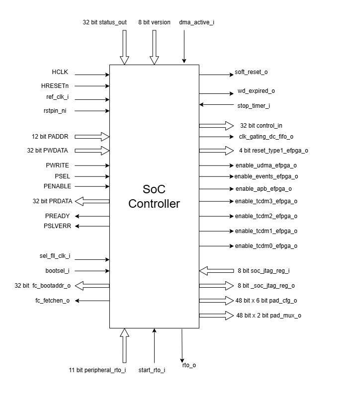
APB SoC Controller Pin Diagram
Clock and Reset
HCLK: APB system clock input; generated by APB PLL.
HRESETn: Active-low system reset signal for initializing CSRs and logic
ref_clk_i: Reference clock input, used for watchdog operations; generated by APB PLL.
soft_reset_o: Soft reset output; triggered by writing to SOFT_RESET CSR.
APB Interface
PADDR[11:0]: APB address bus input
PWDATA[31:0]: APB write data bus input
PWRITE: APB write enable signal
PSEL: APB slave select input
PENABLE: APB enable signal
PRDATA[31:0]: APB read data bus output
PREADY: APB ready signal output, indicates completion of APB transaction
PSLVERR: APB slave error output
Boot and Configuration
sel_fll_clk_i: FLL clock selection input status pin; its value is captured in CLKSEL CSR for monitoring; always high in the current implementation.
bootsel_i: Boot select input status pin; its value is captured in BOOTSEL CSR for monitoring; provided by external device.
fc_bootaddr_o[31:0]: Boot address output for FC (Fabric Controller); controlled via FCBOOT CSR; provided to Core-Complex/Fabric Controller.
fc_fetchen_o: Fetch enable output for FC; controlled via FCFETCH CSR; provided to Core-Complex/Fabric Controller.
dmactive_i: Debug mode active input status pin; its value is captured in BOOTSEL CSR for monitoring.
Watchdog Interface
wd_expired_o: Watchdog expired output signal, triggered when watchdog counter reaches 1;
stoptimer_i: Timer stop input signal; triggered by Core-Complex
rstpin_ni: Active-low reset pin input for resetting watchdog; provided by external device.
Pad Configuration Interface
pad_cfg_o[47:0][5:0]: Pad configuration output signals; controlled via IO_CTRL CSRs or WCFGFUN CSR; provided to I/O mux module.
pad_mux_o[47:0][1:0]: Pad multiplexing output signals; controlled via IO_CTRL CSRs or WCFGFUN CSR; provided to external device.
JTAG Interface
soc_jtag_reg_i[7:0]: JTAG CSR input status pin; its value is captured in JTAGREG CSR for monitoring; always 0 in current implementation.
soc_jtag_reg_o[7:0]: JTAG CSR output; driven by JTAGREG CSR; Not connected in current implementation.
eFPGA Interface
control_in[31:0]: Control output to peripherals; driven by EFPGA_CONTROL CSR
clk_gating_dc_fifo_o: Clock gating for DC FIFO to eFPGA, always 1 as per current implementation
reset_type1_efpga_o[3:0]: Reset signals for eFPGA; driven by RESET_TYPE1_EFPGA CSR
enable_udma_efpga_o: Enable uDMA to eFPGA; driven by ENABLE_IN_OUT_EFPGA CSR
enable_events_efpga_o: Enable events to eFPGA; driven by ENABLE_IN_OUT_EFPGA CSR
enable_apb_efpga_o: Enable APB to eFPGA; driven by ENABLE_IN_OUT_EFPGA CSR
enable_tcdm3_efpga_o: Enable TCDM3 to eFPGA; driven by ENABLE_IN_OUT_EFPGA CSR
enable_tcdm2_efpga_o: Enable TCDM2 to eFPGA; driven by ENABLE_IN_OUT_EFPGA CSR
enable_tcdm1_efpga_o: Enable TCDM1 to eFPGA; driven by ENABLE_IN_OUT_EFPGA CSR
enable_tcdm0_efpga_o: Enable TCDM0 to eFPGA; driven by ENABLE_IN_OUT_EFPGA CSR
status_out[31:0]: Status input signals from eFPGA; its value is captured in EFPGA_STATUS_OUT CSR for monitoring.
version[7:0]: eFPGA version input status pin; its value is captured in EFPGA_VERSION CSR for monitoring.
Ready Timeout Interface
rto_o: Ready timeout output signal provided to Peripheral Interconnect; asserted when ready timeout count reaches 0.
start_rto_i: Start ready timeout input controlled by Peripheral Interconnect; triggers the ready timeout counter.
peripheral_rto_i[10:0]: Peripheral ready timeout input provided by Peripheral Interconnect; indicates which peripheral caused the timeout.