High Level Architecture
The block diagram of the CORE-V-MCU is shown below. Note that the I/O PADs are implementation speific and not considered part of the CORE-V-MCU itself.
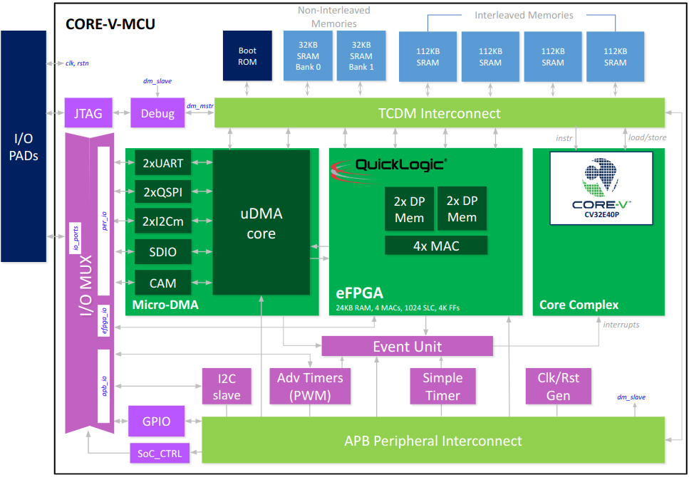
CORE-V-MCU Block Diagram
On-chip Memories
There are four types of on-chip memories visible to the user. These are all accessible to the core, see the Memory Map chapter for addressing information.
Boot ROM
An on-board ROM is provided. The default configuration includes a very simple bootloader, see the CORE-V-MCU Quick Start Guide.
Non-Interleaved SRAM
There are two 32K-byte banks of non-interleaved SRAM, typically used for program store.
Interleaved SRAM
Four 112K-byte banks of interleaved SRAM, typically used for data store. Note that the interleaved addressing is not visible to the user.
DP Memories
The DP memories are accessible by user-defined logic in the eFPGA and are not accessible by the core processor.
Internal Buses
The CORE-V-MCU has two internal bus interconnect fabrics.
TCDM Interconnect
The TCDM Interconnect is a high performance, low latency memory bus interconnect. The core accesses memory (both instruction fetch and data load/stores) via this interconnect. The micro-DMA controller moves data to/from its peripherals into data memory using this bus.
APB Peripheral Interconnect
Many of the peripherals used by the CORE-V-MCU use the APB bus as the control-plane interface. This interconnect is a slave to the TCDM Interconnect and provides the core with memory-mapped access to the CSRs of the APB peripherals. The APB peripherals are:
SoC_CTRL
GPIO
I2C Slave
Advance Timers (PWM)
Event Timers
Clock and Reset Generators
Debug Module
Subsystems
The CORE-V-MCU supports three subsystems
Core Control Subsystem
The core control subsystem accesses the TCDM Interconnect such that it sees all resources of the CORE-V-MCU in a single, flat memory space. The sole component of the core control subsystem is the CV32E40P processor core.
Micro-DMA Subsystem
The micro-DMA (uDMA) manages data transfer to/from memory for a set of peripherals. Its connections to the TCDM Interconnect providing high-bandwidth, low-latency access to the interleaved data memories. Peripherals supported by the uDMA are:
UART
I2C Master
QSPI
SDIO
Camera
Quicklogic Embedded FPGA
The eFPGA connects to the interleaved data memories via the TCDM Interconnect. Note that there are four TCDM buses between the TCDM Interconnect and the eFPGA allowing for eFPGA implementations to support high memory bandwidth requirements.
Other Functional Units
Event Unit
Virtually all peripherals, plus the uDMA and eFPGA subsystem generate signals to commnicate such event as the completion of a data transfer or an error condition. These signals are consolidated by the Event Unit to generate a set of interrupts for the CV32E40P.
IO MUX
To minimize packaging costs, the CORE-V-MCU has fewer top-level I/O signals than required by the total set of peripheral I/O signals. The IO MUX allows the user to select a subset of peripheral I/O to connect to I/O PADs.
JTAG/Debug
CORE-V-MCU supports an industry standard 5-pin JTAG interface supporting RISC-V compliant debug access. Note that the JTAG port does not support any Design For Test features such as logic BIST, logic scan or boundary scan.