UDMA SDIO(SD Input/Output) INTERFACE
The SDIO card provides high speed data I/O with low power consumption for mobile electronic devices. Host devices supporting SDIO can connect the SD slot with I/O devices like Bluetooth, wireless, LAN, GPS Receiver, Digit Camera etc.
Features
It has a clock, command and 4-bit data bus.
Supports quad mode.
Five types of response supported:
No response
48 bits with CRC
48 bits with CRC and BUSY
48 bits with NO CRC
136 bits
Following events are supported:
Error event.
End of transfer event.
Four error status for receive operation
No error
Response timeout
Response wrong direction
Response busy timeout
SDIO operation is synchronized using a sdclk_o clock whose period can be controlled using CLK_DIV CSR.
Block Architecture
uDMA SDIO is a peripheral function of the uDMA subsystem. As such, its CSRs are not directly accessible via the APB bus. Rather, the control plane interface to the uDMA SDIO is managed by the uDMA core within the uDMA subsystem. This is transparent to the programmer, as all uDMA SDIO CSRs appear within the uDMA subsystem’s memory region. As is the case for all uDMA subsystem peripherals, I/O operations are controlled by the uDMA core. This is not transparent to the programmer.
The Figure below is a high-level block diagram of the uDMA SDIO:-
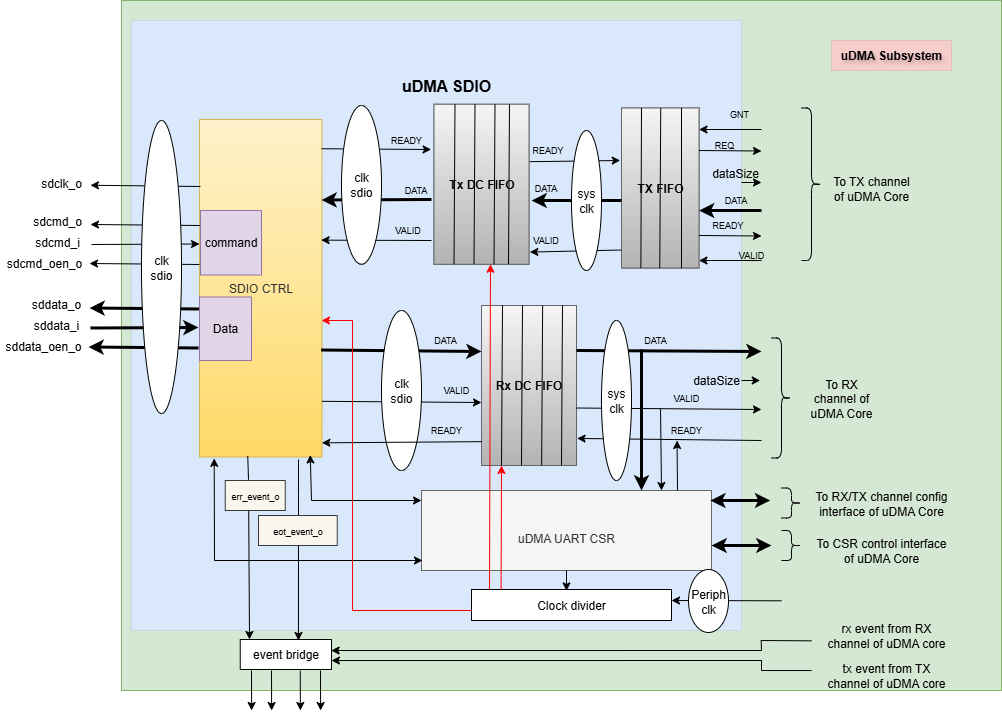
uDMA SDIO Block Diagram
In the block diagram above, the DATA lines are 32 bits wide The DATASIZE pin is 2 bits wide and is currently hardcoded to 0x2. The valid values for the DATASIZE pin are: -
0x0: 1-byte transfer
0x1: 2-byte transfer
0x2: 4-byte transfer
uDMA SDIO uses the Tx channel interface to read the data from the interleaved (L2) memory via the uDMA Core. It transmits the read data to the external SDIO device. uDMA SDIO uses the Rx channel interface to store the data received from the external SDIO device to the interleaved (L2) memory. Refer to uDMA subsystem for more information about the Tx and Rx channel functionality of uDMA Core.
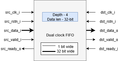
Dual clock FIFO
The uDMA core operates using the system clock, while the uDMA SDIO operates using both the system clock and the peripheral clock. To ensure the uDMA SDIO and core are properly synchronized, dual-clock FIFOs are used in the uDMA SDIO. These are 4-depth FIFOs and can store 32-bit wide data. It is implemented using circular FIFO.
Below diagram shows the interfaces of DC FIFO:
Dual clock FIFO
For Rx operation, source(src_*) interfaces shown in above diagram operate at peripheral clock and destination(dst_*) interfaces operate using system clock.
For Tx operation, source interfaces shown in above diagram operate at system clock and destination interfaces operate using peripheral clock.
Pop operation
The DC FIFO asserts the dst_valid_o (valid) signal to indicate that valid data is available on the data lines. A module waiting for data should read the data lines only when valid pin is high and drive the dst_ready_i (ready) signal to high and reset it in next clock cycle. When DC FIFO receives an active ready signal, indicating that the data has been read, it updates the data lines with new data if FIFO is not empty. If the FIFO is empty, the dst_valid_o signal is deasserted.
Push operation
The DC FIFO asserts the src_ready_o (ready) signal when there is available space to accept incoming data. When an active src_valid_i (valid) signal is received, the data is written into the FIFO. The src_ready_o signal is kept asserted as long as the FIFO has space for more data. IF the DC FIFO is full, push operation will be stalled until the FIFO has empty space and valid line is high. A module transmitting the data to DC FIFO should drive the valid signal low to indicate data lines should not be read.
During SDIO transmit (Tx) operation, the TX DC FIFO is read internally by the SDIO to transmit data to an external device and written by the TX FIFO. During SDIO receive (Rx) operation, the RX DC FIFO is written internally by the SDIO with the data received from the external device and read by the uDMA core.
TX FIFO
uDMA SDIO has a TX FIFO to store the received data from uDMA core. It forwards the data read from L2 memory to the TX DC FIFO. uDMA SDIO on TX path, read the data from TX DC FIFO and transmits it to external device. It is a 2-depth FIFO and can store 32-bit wide data. Below diagram shows the interfaces of TX FIFO:
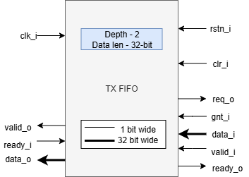
TX FIFO
TX FIFO operates using system clock. clr_i pin is hardcoded with value 0x0.
Pop operation
The read interface of the TX FIFO is connected to the TX DC FIFO. The TX DC FIFO raises ready(ready_i) signal if its FIFO has space. If data is available, TX FIFO asserts the valid_o signal and update the data lines with data. TX FIFO will update the valid signal and data lines at each clock cycle. If the ready signal is high, data lines will be update with new data, otherwise, data lines will show the last transferred byte. If the TX FIFO is empty, the valid_o signal remains deasserted, indicating that no valid data is present on the output lines.
Push operation
The write interface of the TX FIFO is extended to the uDMA Core. The TX FIFO write operation is performed with the help of the req(req_o) and ready(ready_o) signals. The TX FIFO keeps the ready_o (ready) signal high until the TX FIFO is full. TX FIFO raises a req_o signal when it has enough space in FIFO, i.e., ready_o is high, and the pending requests at the uDMA core do not exceed the depth of TX FIFO. TX FIFO receives a GNT (gnt_i) signal from the uDMA core confirming that the request is accepted. TX FIFO maintains a counter to track unserved requests; it applies the following logic to update the counter: -
When a request (req_o) is issued and granted (gnt_i), the TX FIFO increments the counter if either the valid_i or ready_o signal is low.
Regardless of the state of the req_o and gnt_i signals, the frame counter is decremented whenever both valid_i and ready_o are high.
When it receives the valid signal from the uDMA core and the FIFO is not full, the TX FIFO pushes the data coming from the uDMA core. TX tries to read data at each clock cycle until TX FIFO has space and a valid pin is high.
TX FIFO is transparent to users.
Command
SDIO operation begins with the generating of a command. The host can send a command to either a single card or to all connected cards. During the transmit operation, sdcmd_oen_o is pulled low (0) and the command is transferred serially on the sdcmd_o line. The MSB is transmitted first, and the LSB is transmitted last. The direction bit is set to 1, indicating that the command is transmitted from the host to the card.
Bit position |
47 |
46 |
[45:40] |
[39:8] |
[7:1] |
0 |
|---|---|---|---|---|---|---|
Width |
1 |
1 |
6 |
32 |
7 |
1 |
Value |
0 |
1 |
x |
x |
x |
1 |
Description |
Start bit |
Direction bit |
Command opcode |
Command argument |
CRC |
End bit |
The CMD_OP and CMD_ARG CSRs of uDMA SDIO should be used to configure command opcode and command arguments respectively.
When START bit of REG_START CSR is set, the uDMA SDIO will enable the sdclk_o clock. After enabling clocks, uDMA SDIO will drive 0 on sdcmd_oen_o and sdcmd_o to send a start bit.
The command will be send in below sequence : -
Start bit -> Direction bit -> Command opcode -> command arguments -> CRC -> End of transmission
CRC is calculated based on x7+x3+1 polynomial function. CRC will calculated on Command opcode and argument field value.
The uDMA SDIO sends the stop command after sending all the data blocks for multi block transfer. The stop command has fixed command opcode value of 6 and command argument value of 0. Stop command packet is automatically created by SDIO and is transparent to users. The uDMA SDIO reads BLOCK_NUM bit DATA_SETUP CSR to determine the number of blocks to be transferred. In case of multi block transfer, BLOCK_NUM bit DATA_SETUP CSR must be non zero. The stop command will be sent in below sequence: -
Bit position |
47 |
46 |
[45:40] |
[39:8] |
[7:1] |
0 |
|---|---|---|---|---|---|---|
Width |
1 |
1 |
6 |
32 |
7 |
1 |
Value |
0 |
1 |
6’d12 |
32’h0 |
X |
1 |
Description |
Start bit |
Direction bit |
Command opcode |
Command argument |
CRC |
End bit |
After transmitting the stop command, the uDMA SDIO expects RSP_TYPE_48_CRC response from the external device.
Command Response and Data Flow in uDMA SDIO
After sending a command, the uDMA SDIO acts based on the DATA_SETUP CSR and command response settings:
If set for read, it starts a data read (Rx) from the external device (see Data Section), as per the DATA_SETUP CSR.
If configured for a command response, the response is captured and processed (see Response Section).
- If no response is required, or once the response is received:
An End-of-Transfer (EOT) interrupt is triggered.
The uDMA SDIO may then perform a data write (Tx) to the external device(see Data Section), as per the DATA_SETUP CSR.
Response
A response is sent from the external card to the host in reply to a previously received command. During the receive operation, sdcmd_oen_o is pulled high (1), and the response is received serially on the sdcmd_i line. The MSB is read first, and the LSB is read last. The direction bit is set to 0, indicating that the response is transmitted from the card to the host.
The RSP_TYPE bitfield of CMD_OP CSRs can used to configure expected response from the external SDIO device. Following response can be expected from the external device: -
RSP_TYPE_48_CRC, response length will be 38 bit long.
Bit position |
47 |
46 |
[45:40] |
[39:8] |
[7:1] |
0 |
|---|---|---|---|---|---|---|
Width |
1 |
1 |
6 |
32 |
7 |
1 |
Value |
0 |
0 |
x |
x |
x |
1 |
Description |
Start bit |
Direction bit |
Command index |
Card status |
CRC |
End bit |
RSP_TYPE_48_BSY, response length will be 38 bit long.
Bit position |
47 |
46 |
[45:40] |
[39:8] |
[7:1] |
0 |
|---|---|---|---|---|---|---|
Width |
1 |
1 |
6 |
32 |
7 |
1 |
Value |
0 |
0 |
x |
x |
x |
1 |
Description |
Start bit |
Direction bit |
Command index |
Card status |
CRC |
End bit |
RSP_TYPE_48_NOCRC, response length will be 38 bit long.
Bit position |
47 |
46 |
[45:40] |
[39:8] |
[7:1] |
0 |
|---|---|---|---|---|---|---|
Width |
1 |
1 |
6 |
32 |
7 |
1 |
Value |
0 |
0 |
x |
x |
1111111 |
1 |
Description |
Start bit |
Direction bit |
Command index |
Card status |
Reserved |
End bit |
RSP_TYPE_136, response length will be 134 bit long.
Bit position |
135 |
134 |
[133:128] |
[127:1] |
0 |
|---|---|---|---|---|---|
Width |
1 |
1 |
6 |
127 |
1 |
Value |
0 |
0 |
111111 |
x |
1 |
Description |
Start bit |
Direction bit |
Reserved |
Response content including CRC |
End bit |
If any of the above response is selected via RSP_TYPE bitfield of CMD_OP CSRs then the uDMA SDIO will wait for a response after sending command. To receive response, uDMA QSPI drives sdcmd_oen_o with value 1 and expects sdcmd_i pin to have value 0(indicating start bit) within 38 clock cycles. If uDMA SDIO does not receive response from the external device within 38 sdclk_o clock cycle, it updates the command STATUS to STATUS_RSP_TIMEOUT and does not wait for the response. If command response is received successfully, uDMA SDIO validates if the direction bit received at sdcmd_i pin. If the value at the sdcmd_i pin is non-zero then it updates the command STATUS to STATUS_RSP_WRONG_DIR. After validating direction, uDMA SDIO will read data up to response length. If Response expects the CRC value then uDMA SDIO reads the command CRC and perform CRC validation. In case of RSP_TYPE_48_BSY response, the uDMA SDIO expects that data lines to be inactive, if not, uDMA SDIO retry after 8 clock cycles to confirm whether data lines are free or not. If the data lines are busy even after 8 clock cycles then SDIO updates the command STATUS to STATUS_RSP_BUSY_TIMEOUT. The SDIO, irrespective of whether data lines are busy or not spends 8 clock cycle before raising eot interrupt. Apart from asserting EOT interrupt , the uDMA SDIO enable SDIO to perform data write (Tx) operation to the external device.
CRC is calculated based on x7+x3+1 polynomial function.
The response data can be read from REG_RSPx{x = 0 to 3} CSR of SDIO.
Data
Data can be transferred from the external device to the host uDMA SDIO or vice versa. It is transferred via the data lines.
Data transfer to/from the host is done in blocks. Data blocks are succeeded by CRC bits.
Tx operation
The uDMA SDIO can be configured to perform Tx operation based on the below conditions:
When command response is needed - RWN bit of DATA_SETUP CSR is 0 and EN bit of DATA_SETUP CSR is 1 and command response is received.
When command response is not needed - RWN bit of DATA_SETUP CSR is 0 and EN bit of DATA_SETUP CSR is 1 and command is sent.
To initiate Tx operation, uDMA sdio will drive 1 on sddata_oen_o line. Data will be transmitted over sddata_o data lines in below sequence: -
Start bit -> Data -> CRC - > End
To send start bit, the uDMA SDIO will drive the sddata_o with value 0. CRC for Tx operation is calculated based on x16+x12+x5+1 polynomial function. CRC is calculated by the SDIO on the data received from the L2 memory.
To get transmit data from L2 memory TX FIFO requests data from the uDMA core by asserting both the READY (space available) and REQ (request a new transaction) signals. The uDMA core arbitrates among multiple peripherals on receiving the REQ signal. When the SDIO TX channel is enabled and wins arbitration, the uDMA core issues a GNT (grant) signal and places the valid data read from L2 memory on the bus along with asserting VALID signal. Tx FIFO stores this received data and keeps the READY and REQ signals asserted as long as the aforementioned conditions remain valid. The uDMA core de-asserts the VALID signal in the following clock cycle and reasserts it only when new data is available for transmission. Initially, after reset or power-up, READY/REQ are asserted since the FIFO is empty.
Whenever TX FIFO has valid data and the TX DC FIFO has shown readiness to accept data by asserting READY signal, it asserts VALID signal and update the data lines of DC FIFO with the valid data. The data transmission from TX FIFO to TX DC FIFO is synchronized using system clock. TX DC FIFO de-asserts READY when it is full, temporarily stalling the upstream TX FIFO. Once space is freed, READY is re-asserted. Data moves from TX FIFO to TX DC FIFO when both VALID and READY are high on the same cycle.
The uDMA SDIO must be configured using the TX_SADDR, TX_SIZE and TX_CFG CSRs to read transmit data from L2 memory.
Rx Operation
Rx operation is initiated when RWN and EN bit of DATA_SETUP CSR is 1 and command is sent. The uDMA SDIO receives data on the sddata_i data lines. Data will be received over sddata_i data lines in below sequence: -
Start bit -> Data -> CRC - > End
To receive response, uDMA QSPI expects sddata_i pin to have value 0(indicating start bit) within BLOCK_NUM clock cycles. If uDMA SDIO does not receive response from the external device within BLOCK_NUM sdclk_o clock cycle, it updates the Rx STATUS to STATUS_RSP_TIMEOUT and does not wait for the response. After successfully receiving the start bit, it reads BLOCK_SIZE data and 16 bit crc values. After successfully reading BLOCK_NUM data and subsequent crc bits, uDMA SDIO sets the EOT bit of STATUS CSR. Reading EOT bit will clear it. The uDMA SDIO reads the start bit, BLOCK_SIZE data and 16 bit crc values for BLOCK_NUM to complete Rx operation.
The uDMA SDIO pushes each BLOCK_SIZE data and CRC into the RX DC FIFO. The uDMA SDIO when it has data asserts the valid lines of RX DC FIFO. RX DC FIFO reads the data lines and asserts the valid lines for uDMA core to indicate the availability of new data.
To store the received data into L2 memory, the uDMA SDIO must be programmed with RX_SADDR, RX_SIZE and RX_CFG CSRs.
On detecting the valid signal, the uDMA core arbitrates for access. If the uDMA SDIO RX channel wins the arbitration and the core’s RX FIFO has space, uDMA core asserts READY, latching the data from RX DC FIFO. The data is then written into L2 memory at the address specified by RX_SADDR, with automatic increment for subsequent bytes. The cycle repeats until the entire transfer (as defined by RX_SIZE) completes.
CRC for both Rx and Tx operation is calculated based on x16+x12+x5+1 polynomial function.
Note
The uDMA SDIO module does not support CRC error detection for externally received command responses or data.
Interrupt
uDMA SDIO generates the following interrupts:
Error interrupt: Raised by uDMA SDIO when it encounter timeout error while performing command-response reception or Rx operation.
End of transfer interrupt: Raised by uDMA SDIO after successfully completing Rx/Tx operation.
Rx channel interrupt: Raised by uDMA core’s Rx channel after pushing the last byte of RX_SIZE bytes into core RX FIFO.
Tx channel interrupt: Raised by uDMA core’s Tx channel after pushing the last byte of TX_SIZE bytes into core TX FIFO.
The RX and TX channel interrupts are cleared by the uDMA core if any of the following conditions occur:
If a clear request for the RX or TX uDMA core channel is triggered via the CLR bitfield in the respective RX or TX CFG CSR of the uDMA SDIO.
If either the RX or TX uDMA channel is disabled via the CFG CSR of the uDMA SDIO, or if access is not granted by the uDMA core’s arbiter.
If continuous mode is enabled for the RX or TX uDMA channel through the CFG CSR of the SDIO uDMA.
RX and TX channel interrupts are transparent to users.
The event bridge forwards interrupts over dedicated lines to the APB event controller for processing. Each interrupt has its own dedicated line. Users can mask these interrupts through the APB event controller’s control and status registers (CSRs).
System Architecture
The figure below shows how the uDMA SDIO interfaces with the rest of the CORE-V-MCU components and the external SDIO device:-
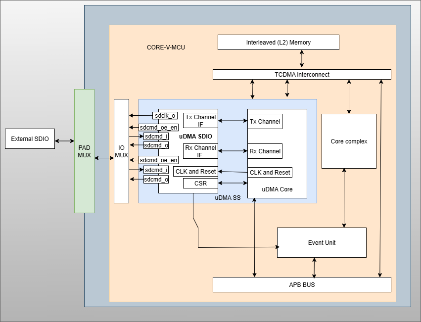
uDMA SDIO CORE-V-MCU connection diagram
Programming Model
As with most peripherals in the uDMA Subsystem, software configuration for the uDMA SDIO interface can be conceptualized into three key steps:
I/O Configuration: Set up external clock and chip select and output enable lines.
uDMA core Setup: Configure source/destination addresses, transfer size, and direction for TX and RX operation using channel CSRs. This enables efficient data movement from L2 memory to SDIO via uDMA core. Update the L2 memory with command sequence to configure SDIO controller.
Data Transfer Management: Read command sequence from L2 memory to configure SDIO for RX/TX operation. Drive SDIO bus based on the received command sequence.
Refer to the Firmware Guidelines section in the current chapter for more information.
uDMA SDIO CSRs
Refer to Memory Map for peripheral domain address of the uDMA SDIO.
NOTE: Several of the uDMA SDIO CSRs are volatile, meaning that their read value may be changed by the hardware. For example, writing the RX_SADDR CSR will set the address of the receive buffer pointer. As data is received, the hardware will update the value of the pointer to indicate the current address. As the name suggests, the value of non-volatile CSRs is not changed by the hardware. These CSRs retain the last value written by software.
A CSR’s volatility is indicated by its “type”.
Details of CSR access type are explained here.
The CSRs RX_SADDR and RX_SIZE specify the configuration for the transaction on the RX channel. The CSRs TX_SADDR and TX_SIZE specify the configuration for the transaction on the TX channel. The uDMA Core creates a local copy of this information at its end and uses it for current ongoing transactions.
RX_SADDR
Offset: 0x0
Type: volatile
Field |
Bits |
Access |
Default |
Description |
|---|---|---|---|---|
SADDR |
18:0 |
RW |
0x0 |
Address of the Rx buffer. This is location in the L2 memory where SDIO will write the received data. Read & write to this CSR access different information. On Write: Address of Rx buffer for next transaction. It does not impact current ongoing transactions. On Read: Address of read buffer for the current ongoing transaction. This is the local copy of information maintained inside the uDMA core. |
RX_SIZE
Offset: 0x04
Type: volatile
Field |
Bits |
Access |
Default |
Description |
|---|---|---|---|---|
SIZE |
19:0 |
RW |
0x0 |
Size of Rx buffer (amount of data to be transferred by SDIO to L2 memory). Read & write to this CSR access different information. On Write: Size of Rx buffer for next transaction. It does not impact current ongoing transaction. On Read: Bytes left for current ongoing transaction. This is the local copy of information maintained inside the uDMA core. |
RX_CFG
Offset: 0x08
Type: volatile
Field |
Bits |
Access |
Default |
Description |
|---|---|---|---|---|
CLR |
6:6 |
WO |
0x0 |
Clear the local copy of Rx channel configuration CSRs inside uDMA core |
PENDING |
5:5 |
RO |
0x0 |
|
EN |
4:4 |
RW |
0x0 |
Enable the Rx channel of the uDMA core to perform Rx operation |
CONTINUOUS |
0:0 |
RW |
0x0 |
|
TX_SADDR
Offset: 0x10
Type: volatile
Field |
Bits |
Access |
Default |
Description |
|---|---|---|---|---|
SADDR |
18:0 |
RW |
0x0 |
Address of the Tx buffer. This is location in the L2 memory from where SDIO will read the data to transmit. Read & write to this CSR access different information. On Write: Address of Tx buffer for next transaction. It does not impact current ongoing transactions. On Read: Address of Tx buffer for the current ongoing transaction. This is the local copy of information. maintained inside the uDMA core. |
TX_SIZE
Offset: 0x14
Type: volatile
Field |
Bits |
Access |
Default |
Description |
|---|---|---|---|---|
SIZE |
19:0 |
RW |
0x0 |
Size of Tx buffer (amount of data to be read by SDIO from L2 memory for Tx operation). Read & write to this CSR access different information. On Write: Size of Tx buffer for next transaction. It does not impact current ongoing transactions. On Read: Bytes left for current ongoing transaction, i.e., bytes left to read from L2 memory. This is the local copy of information maintained inside the uDMA core. |
TX_CFG
Offset: 0x18
Type: volatile
Field |
Bits |
Access |
Default |
Description |
|---|---|---|---|---|
CLR |
6:6 |
WO |
0x0 |
Clear the local copy of Tx channel configuration CSRs inside uDMA core |
PENDING |
5:5 |
RO |
0x0 |
|
EN |
4:4 |
RW |
0x0 |
Enable the transmit channel of uDMA core to perform Tx operation |
CONTINUOUS |
0:0 |
RW |
0x0 |
|
CMD_OP
Offset: 0x20
Type: non-volatile
Field |
Bits |
Access |
Default |
Description |
|---|---|---|---|---|
OP |
13:8 |
W |
0x00 |
Operation code specifying the command or function to be performed. This 6-bit field selects the type of operation initiated by the controller or processor. |
RSP_TYPE |
2:0 |
W |
0x0 |
Response type expected for the issued operation. This 3-bit field defines the format or presence of the response data.
|
CMD_ARG
Offset: 0x24
Type: non-volatile
Field |
Bits |
Access |
Default |
Description |
|---|---|---|---|---|
ARG |
31:0 |
W |
0x00000000 |
Argument value associated with the command operation. This 32-bit field provides optional or required data used by the command specified in the OP field. The meaning of this field depends on the command type and context. |
DATA_SETUP
Offset: 0x28
Type: non-volatile
Field |
Bits |
Access |
Default |
Description |
|---|---|---|---|---|
BLOCK_SIZE |
25:16 |
W |
0x000 |
Specifies the size of each data block to be transferred, in bytes. Typically used to define the transfer chunk size for multi-block operations. |
BLOCK_NUM |
15:8 |
W |
0x00 |
Number of blocks to be transferred. This value works together with BLOCK_SIZE to determine total transfer size.
|
QUAD |
2:2 |
W |
0x0 |
Enables Quad SPI mode when set to 1. In this mode, 4 data lines are used for faster data transfer. Set to 0 for standard mode. |
RWN |
1:1 |
W |
0x0 |
Read/Write control: 0 indicates a write operation, 1 indicates a read operation. |
EN |
0:0 |
W |
0x0 |
Enable bit. When set to 1, triggers the start of the read-write operation. Read-write is decided based on the RWN bitfield. |
REG_START
Offset: 0x2C
Type: non-volatile
Field |
Bits |
Access |
Default |
Description |
|---|---|---|---|---|
START |
0:0 |
W |
0x0 |
Start bit. Writing 1 to this bit initiates the command transmit operation |
REG_RSP0
Offset: 0x30
Type: volatile
Field |
Bits |
Access |
Default |
Description |
|---|---|---|---|---|
DATA |
31:0 |
R |
0x0 |
Represents the 31:0 bits of RSP data |
REG_RSP1
Offset: 0x34
Type: volatile
Field |
Bits |
Access |
Default |
Description |
|---|---|---|---|---|
DATA |
31:0 |
R |
0x0 |
Represents the 63:32 bits of RSP data |
REG_RSP2
Offset: 0x38
Type: volatile
Field |
Bits |
Access |
Default |
Description |
|---|---|---|---|---|
DATA |
31:0 |
R |
0x0 |
Represents the 95:64 bits of RSP data |
REG_RSP3
Offset: 0x3C
Type: volatile
Field |
Bits |
Access |
Default |
Description |
|---|---|---|---|---|
DATA |
31:0 |
R |
0x0 |
Represents the 127:96 bits of RSP data |
CLK_DIV
Offset: 0x40
Type: non-volatile
Field |
Bits |
Access |
Default |
Description |
|---|---|---|---|---|
DIV_VALID |
8:8 |
RW |
0x0 |
Indicates whether the value in DIV_DATA is valid. When set to 1, the divider logic uses the value in DIV_DATA. When 0, the divider is considered inactive or disabled. |
DIV_DATA |
7:0 |
RW |
0x0 |
8-bit divider value to be used when DIV_VALID is set. This value typically controls the clock division ratio or timing behavior of a functional block. |
STATUS
Offset: 0x44
Type: volatile
Field |
Bits |
Access |
Default |
Description |
|---|---|---|---|---|
STATUS |
31:16 |
R |
0x0 |
|
ERR |
1:1 |
RWC |
0x0 |
Writing any value clears the bit. Indicates error either during data or command-response reception. Error type can be read from the status bit(31:16)
|
EOT |
0:0 |
RWC |
0x0 |
Writing any value clears the bit.
|
Firmware Guidelines
Clock Enable, Reset & Configure uDMA SDIO
- Configure uDMA Core’s PERIPH_CLK_ENABLE to enable uDMA SDIO’s peripheral clock. A peripheral clock is used by uDMA SDIO to synchronize data with external device.
Configure uDMA SDIO’s CLK_DIV CSR to update the period of SDIO’s peripheral clock. Refer to the register description for more information.
- Configure uDMA Core’s PERIPH_RESET CSR to issue a reset signal to uDMA QSPI. The uDMA QSPI can be reset via:
System system
Setting corresponding bit in the uDMA Core’s PERIPH_RESET CSR
Command
Configure CMD_OP with command opcode and response type expected after transmitting command to the external device.
Configure CMD_ARG with the argument associated with the command opcode selected via CMD_OP bitfield.
Configure REG_START CSR to initiate command transfer from SDIO to the external device.
if RSP_TYPE bitfield is configured with response type then REG_RSPx{x = 0 to 3} shall be read to get the received response from the external device.
Tx Operation
Configure the TX channel using the TX_CFG CSR. Refer to the CSR details for detailed information.
- For each transaction:
Update uDMA SDIO’s TX_SADDR CSR with an interleaved (L2) memory address. SDIO will read the data from this memory address for transmission.
Configure the uDMA SDIO’s TX_SIZE CSR with the size of data that the SDIO needs to transmit. uDMA SDIO will copy the transmit TX_SIZE bytes of data from the TX_SADDR location of interleaved memory.
Configure DATA_SETUP setup CSR to enable transmit of data from the L2 memory to the external. The Tx operation will start only after successfully command transfer. Refer to the DATA_SETUP CSR for more information.
The uDMA SDIO can be configured to perform Tx operation based on the below conditions:
When command response is needed - RWN bit of DATA_SETUP CSR is 0 and EN bit of DATA_SETUP CSR is 1 and command response is received.
When command response is not needed - RWN bit of DATA_SETUP CSR is 0 and EN bit of DATA_SETUP CSR is 1 and command already transferred.
Of course, the command should be transferred successfully for Tx operation to start.
Rx Operation
Configure the RX channel using the RX_CFG CSR. Refer to the CSR details for detailed information.
- For each transaction:
Update uDMA SDIO’s RX_SADDR CSR with an interleaved (L2) memory address. SDIO will write the data to this memory address for transmission.
Configure uDMA SDIO’s RX_SIZE CSR with the size of data that SDIO needs to transmit. uDMA SDIO will copy the transmit RX_SIZE bytes of data to the RX_SADDR location of interleaved memory.
Configure DATA_SETUP setup CSR to enable transmission of data from the external device to L2 memory. The Rx operation will start only after a successful command transfer. Refer to the DATA_SETUP CSR for more information. Refer to the DATA_SETUP CSR for more information.
The uDMA SDIO can be configured to perform Tx operation based on the below conditions: - Rx operation is initiated when RWN and EN bit of DATA_SETUP CSR is 1 and command is already transferred.
STATUS bit of the STATUS CSR reflects the status of Rx operation.
Of course, the command should be transferred successfully for Rx operation to start.
End of transfer Interrupt
The uDMA SDIO asserts end of transmission event when it completes either Tx or Rx operation. EOT bit of STATUS CSR reflects the error status. The end of transfer interrupt is automatically cleared in the next clock cycle.
Error interrupt
The uDMA SDIO asserts error event when it faces an error during either reception of command-response or data from the external device. ERR bit of STATUS CSR reflects the error status. The error interrupt is automatically cleared in the next clock cycle.
Pin Diagram
The Figure below is a high-level block diagram of the uDMA: -
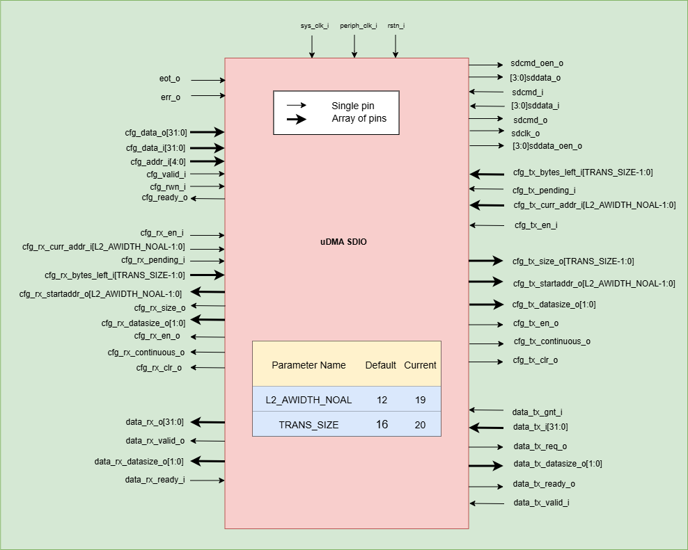
uDMA SDIO Pin Diagram
Below is a categorization of these pins:
Tx channel interface
The following pins constitute the Tx channel interface of uDMA SDIO. uDMA SDIO uses these pins to read data from interleaved (L2) memory:
data_tx_req_o
data_tx_gnt_i
data_tx_datasize_o
data_tx_i
data_tx_valid_i
data_tx_ready_o
Data_tx_datasize_o pin is hardcoded to value 0x0. These pins reflect the configuration values for the next transaction.
Rx channel interface
The following pins constitute the Rx channel interface of uDMA SDIO. uDMA SDIO uses these pins to write data to interleaved (L2) memory:
data_rx_datasize_o
data_rx_o
data_rx_valid_o
data_rx_ready_i
data_rx_datasize_o pin is hardcoded to value 0x0. These pins reflect the configuration values for the next transaction.
Clock interface
sys_clk_i
periph_clk_i
uDMA CORE derives these clock pins. periph_clk_i is used to calculate baud rate. sys_clk_i is used to synchronize SDIO with uDAM Core.
Reset interface
rstn_i
uDMA core issues reset signal to SDIO using reset pin. This is active low signal.
uDMA SDIO bus interface
command interface
sdcmd_o
sdcmd_i
sdcmd_oen_o
sdcmd_oen_o is an active low signal. It is enabled during transfer of command and is disabled during reception of response.
data interface
sddata_o
sddata_i
sddata_oen_o
sddata_oen_o is an active low signal. It is enabled during transfer of command and is disabled during reception of response.
sdio clock
sdclk_o
uDMA SDIO interface to generate interrupt
eot_o
err_o
eot_o interrupt is generated at the end of receive or transmit operation. `err_o`interrupt is generated when an error is observed during receive operation. These are active high signal.
uDMA SDIO interface to read-write CSRs
The following interfaces are used to read and write to SDIO CSRs. These interfaces are managed by uDMA Core:
cfg_data_i
cfg_addr_i
cfg_valid_i
cfg_rwn_i
cfg_ready_o
cfg_data_o
uDMA SDIO Rx channel configuration interface
uDMA SDIO uses the following pins to share the value of config CSRs, i.e., RX_SADDR, RX_SIZE, and RX_CFG, with the uDMA core: -
cfg_rx_startaddr_o
cfg_rx_size_o
cfg_rx_datasize_o
cfg_rx_continuous_o
cfg_rx_en_o
cfg_rx_clr_o
The cfg_rx_datasize_o pin is stubbed.
SDIO shares the values present over the below pins as read values of the config CSRs, i.e. RX_SADDR, RX_SIZE, and RX_CFG:
cfg_rx_en_i
cfg_rx_pending_i
cfg_rx_curr_addr_i
cfg_rx_bytes_left_i
These values are updated by the uDMA core and reflect the configuration values for the current ongoing transactions.
uDMA SDIO Tx channel configuration interface
uDMA SDIO uses the following pins to share the value of config CSRs, i.e., TX_SADDR, TX_SIZE, and TX_CFG, with the uDMA core: -
cfg_tx_startaddr_o
cfg_tx_size_o
cfg_tx_datasize_o
cfg_tx_continuous_o
cfg_tx_en_o
cfg_tx_clr_o
The cfg_tx_datasize_o pin is stubbed.
SDIO shares the values present over the below pins as read values of the config CSRs, i.e., TX_SADDR, TX_SIZE, and TX_CFG:
cfg_tx_en_i
cfg_tx_pending_i
cfg_tx_curr_addr_i
cfg_tx_bytes_left_i
These values are updated by the uDMA core and reflect the configuration values for the current ongoing transactions.