APB I2C SLAVE
The I2C slave enables the CORE-V-MCU to interact with an external I2C master device by responding to transactions on an I2C bus.
Features
Supports RX/TX operation with external I2C master device
Bidirectional communication between I2C and APB interfaces
Configurable I2C device address (7-bit)
- Adjustable timing parameters for I2C operation:
Debounce length
SCL delay length
SDA delay length
- Dual communication modes:
Single-byte messaging with status tracking
FIFO-based data transfer for bulk transfer (up to 256 bytes in each direction)
- Comprehensive interrupt support:
Programmable interrupt conditions based on FIFO status flags
Separate interrupt paths for I2C and APB interfaces
- FIFO management features:
256-byte FIFO depth for each direction
Read and write flags to monitor FIFO status.
FIFO flush capability
I2C operations enable/disable control
Block Architecture
I2C slave contains I2C slave interface and APB slave interface. There are FIFOs and CSRs for handling communication with external I2C controllers.
The figure below is a high-level block diagram of the I2C Slave:-
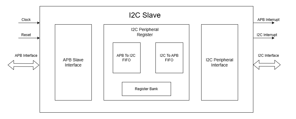
I2C Slave Block Diagram
Below is a brief description of the 3 sub-modules:
APB Slave Interface
Responsible for APB communication: passing information to and from the I2C CSR module through the APB interface. It handles the APB protocol, including address decoding, data transfer, and control signal generation.
I2C Peripheral CSR
The I2C peripheral CSR houses the CSRs of the I2C Slave and drives the interrupt port for APB and I2C. The CSRs are common to both the APB and I2C interfaces. The Firmware can access theses CSRs via the APB interface and the external I2C master can access them via the I2C interface. The CSRs manage the I2C device address, enabling/disabling the I2C slave, and configuring timing parameters for I2C operations and FIFO management. The external I2C master needs to access the CSRs for different parameters related to transmitting such as interrupt configuration, checking FIFO status, and reading/writing data. Please refer to the I2C Slave CSRs section below for a detailed description of the CSRs.
This module also instantiates two FIFOs:
FIFO_sync_256x8_i2c_to_apb: Transfers data from I2C to APB.
FIFO_sync_256x8_apb_to_i2c: Transfers data from APB to I2C.
Both FIFOs are 256 bytes deep and 8 bits wide, allowing for efficient burst data transfer between the I2C and APB interfaces.
I2C Slave Interface
It handles all I2C protocol operations, including detecting start and stop conditions, address recognition, data transmission and reception, sending ACK/NACK signals, and managing the timing of the SDA (Serial Data) and SCL (Serial Clock) lines with built-in line filtering. Communication with the external I2C master occurs over these two lines, forming the I2C bus. The module exchanges information with the internal I2C Peripheral CSR block and drives or samples data on the SDA line in coordination with SCL timing, in response to master requests.
Note: In I2C Slave module the SDA line is divided into 3 signals -
i2c_sda_i: Carries the input data from the I2C master to the slave.
i2c_sda_o: Carries the output data from the slave to the I2C master.
i2c_sda_oe: Output enable signal that indicates when i2c_sda_o is actively driving the SDA line. This signal is asserted (high) when the slave is transmitting data.
Relationship Between I2C and APB Interfaces
The role of both the I2C and the APB interfaces is to handle their respective communication protocols and facilitate data transfer between the I2C master and the APB master (CORE-V-MCU Core-Complex) through the CSRs housed in the I2C Peripheral CSR block.
I2C Device Address
The I2C slave device address is a 7-bit address that identifies the slave device on the I2C bus.
The I2C slave module allows the configuration of this address through the I2CS_DEV_ADDRESS CSR.
When an I2C master sends a START condition followed by the device address, the I2C slave checks if the received address matches the configured address in CSR.
If it matches, the I2C slave acknowledges the address and proceeds with the transaction; otherwise, it ignores the transaction and remains idle.
I2C Signals Processing
Debounce Length
The I2C slave module includes a debounce mechanism to filter out noise on the SDA and SCL lines.
Debouncing is the process of ensuring that a signal is stable before it is considered valid i.e., it prevents false triggering due to noise or glitches on the I2C lines.
It is particularly important in I2C communication, where the SDA and SCL lines can be susceptible to noise, especially in electrically noisy environments.
The debounce length is configurable through the `I2CS_DEBOUNCE_LENGTH CSR, which specifies the number of system clock cycles over which the I2C lines should be debounced.
Note: In the current implementation the debounce length is not used.
SCL and SDA Delay Length
Delay length is the sampling rate of the SCL and SDA lines, this is used to filter out noise on the I2C lines.
The I2C slave uses counters that count up to these delay values at every clock cycle before sampling the SCL and SDA lines. Only when the counter reaches the specified delay length does it take a new sample of the respective I2C line.
If the SCL or SDA line remain stable for 3 consecutive samples, the I2C slave considers the line stable and valid for processing.
This creates a low-pass filtering effect that removes high-frequency noise while preserving the actual I2C signal transitions.
The SCL and SDA length can be configured through the I2CS_SCL_DELAY_LENGTH and I2CS_SDA_DELAY_LENGTH CSRs respectively.
- Configuration:
Shorter delay lengths = faster sampling = less filtering (suitable for clean, high-speed buses)
Longer delay lengths = slower sampling = more filtering (suitable for noisy environments or slower I2C speeds)
Communication Between I2C Slave and external I2C master
The I2C Slave module facilitates seamless communication between the I2C Slave and external I2C master device, enabling data exchange in both single-byte and burst modes. The communication is managed through FIFOs and CSRs, ensuring efficient and reliable data transfer.
I2C Slave Single-Byte TX Operation flow
APB master writes data to
MSG_APB_TO_I2CCSR.Status bit in
MSG_APB_TO_I2C_STATUSCSR is set by hardware.Output interrupt
i2c_interrupt_ois raised to the external device if the interrupt is enabled in theI2C_INTERRUPT_ENABLECSR and associated bit inI2C_INTERRUPT_STATUSis set.I2C master initiates a read request over the bus with the address of
MSG_APB_TO_I2C CSR, requesting the data of the CSR.I2C slave, if enabled via I2CS_ENABLE CSR, responds to this request by retrieving the data from the
MSG_APB_TO_I2CCSR and putting it on the I2C bus, delivering it to the external I2C master.Status bit in
MSG_APB_TO_I2C_STATUSandI2C_INTERRUPT_STATUSis cleared by hardware and thei2c_interrupt_osignal is lowered.
I2C Slave Single-Byte RX Operation flow
I2C master initiates a write request with the addrress of
MSG_I2C_TO_APBCSR and the data to be written.I2C slave, if enabled via I2CS_ENABLE CSR, retrives the CSR address and data from the APB bus and writes it to the respective CSR(
MSG_I2C_TO_APBCSR in this case).Status bit in
MSG_I2C_TO_APB_STATUSCSR is set by hardware.Output interrupt
apb_interrupt_ois raised if the interrupt is enabled in theAPB_INTERRUPT_ENABLECSR and associated bit inAPB_INTERRUPT_STATUSis set.APB master reads
MSG_I2C_TO_APBCSR to retrieve data.Status bit in
MSG_I2C_TO_APB_STATUSandAPB_INTERRUPT_STATUSis cleared by hardware and theapb_interrupt_osignal is lowered.
I2C Slave FIFO-Based Multi-Byte TX Operation flow
APB master writes data to
FIFO_APB_TO_I2C_WRITE_DATA_PORTCSR.The data is pushed in the APB to I2C FIFO by the hardware.
FIFO status is reflected in
FIFO_APB_TO_I2C_WRITE_FLAGSCSR.
i2c_interrupt_ointerrupt can be generated based on FIFO status and interrupt configuration.External I2C master initiates a read request over the bus with the address of
FIFO_APB_TO_I2C_READ_DATA_PORTCSR, requesting the data of the CSR.I2C slave, if enabled via I2CS_ENABLE CSR, responds to this request by retrieving the data from the
FIFO_APB_TO_I2C_READ_DATA_PORTCSR and putting it on the I2C bus, delivering it to the external I2C master.The data is popped from the APB to I2C FIFO by the hardware and the interrupt will be cleared.
FIFO status is updated in
FIFO_APB_TO_I2C_READ_FLAGSCSR.
I2C Slave FIFO-Based Multi-Byte RX Operation flow
External I2C master initiates a write request with the addrress of
FIFO_I2C_TO_APB_WRITE_DATA_PORTCSR and the data to be written.I2C slave, if enabled via I2CS_ENABLE CSR, retrives the CSR address and data from the bus and writes it to the respective CSR(
FIFO_I2C_TO_APB_WRITE_DATA_PORTCSR in this case).The data is pushed in the I2C to APB FIFO by the hardware.
FIFO status is reflected in
FIFO_I2C_TO_APB_WRITE_FLAGSCSR.
apb_interrupt_ointerrupt can be generated based on FIFO status and interrupt configuration.APB master reads data from
FIFO_I2C_TO_APB_READ_DATA_PORTCSR.The data is popped from the I2C to APB FIFO by the hardware and the interrupt will be cleared.
FIFO status is updated in
FIFO_I2C_TO_APB_READ_FLAGSCSR.
Note: Refer to the I2C states section below for a detailed understanding of I2C operations.
Flags and Interrupts
The I2C Slave module uses flags and interrupts to ensure efficient communication and prevent data loss:
- Read Flags:
Indicate the number of items present in the FIFO.
Accessible through
FIFO_I2C_TO_APB_READ_FLAGS(for single-byte reception) andFIFO_APB_TO_I2C_READ_FLAGS(for multi-byte reception) CSRs.
- Write Flags:
Indicate the available space in the FIFO.
Accessible through
FIFO_I2C_TO_APB_WRITE_FLAGS(for single-byte reception) andFIFO_APB_TO_I2C_WRITE_FLAGS(for multi-byte reception) CSRs.
- Interrupts:
Generated based on FIFO thresholds or new message availability for both APB and I2C master through dedicated interrupt signals.
Configurable through
I2C_INTERRUPT_ENABLEandAPB_INTERRUPT_ENABLECSRs.Status can be monitored using
I2C_INTERRUPT_STATUSandAPB_INTERRUPT_STATUSCSRs.
Refer to the respective CSRs for detailed descriptions of the flags and interrupt configurations.
Interrupts
The I2C Slave module provides comprehensive interrupt support for both the I2C and APB interfaces. These interrupts are designed to notify the respective masters about specific events or conditions, ensuring efficient communication and data handling.
I2C Interface Interrupts
The i2c_interrupt_o signal is asserted for the external I2C master device to notify of specific coniditons being met. The following conditions can trigger this interrupt:
Availability of a new single-byte message from the APB to the I2C interface via MSG_APB_TO_I2C CSR.
Write flags of the I2C-to-APB FIFO reaching specific levels configured via INTERRUPT_FIFO_I2C_TO_APB_WRITE_FLAGS_SELECT CSR, indicating available space in the FIFO.
Read flags of the APB-to-I2C FIFO reaching specific levels configured via INTERRUPT_FIFO_I2C_TO_APB_READ_FLAGS_SELECT CSR, indicating pending data for the I2C master to process.
The i2c_interrupt_o signal is deasserted once the external I2C master has performed the necessary read/write operations to clear the underlying interrupt condition(message availability, read flags, write flags).
APB Interface Interrupts
The apb_interrupt_o signal is asserted for the CORE-V-MCU Core-Complex to notify of specific coniditons being met. The following conditions can trigger this interrupt:
Availability of a new single-byte message from the I2C to the APB interface via MSG_I2C_TO_APB CSR.
Write flags of the APB-to-I2C FIFO reaching specific levels configured via INTERRUPT_FIFO_APB_TO_I2C_WRITE_FLAGS_SELECT CSR, indicating available space in the FIFO.
Read flags of the I2C-to-APB FIFO reaching specific levels configured via INTERRUPT_FIFO_APB_TO_I2C_READ_FLAGS_SELECT CSR, indicating pending data for the APB master to process.
The apb_interrupt_o signal is deasserted once the CORE-V-MCU Core-Complex has performed the necessary read/write operations to clear the interrupt condition(message availability, read flags, write flags).
Interrupt Configuration and Handling
Interrupts can be enabled or disabled through the
I2C_INTERRUPT_ENABLEandAPB_INTERRUPT_ENABLECSRs for external I2C master and core-complex respectively.The interrupt status can be monitored using the
I2C_INTERRUPT_STATUSandAPB_INTERRUPT_STATUSCSRs for external I2C master and core-complex respectively.Specific interrupt conditions for FIFO read and write flags can be configured using the
INTERRUPT_FIFO_I2C_TO_APB_*_FLAGS_SELECTandINTERRUPT_FIFO_APB_TO_I2C_*_FLAGS_SELECTCSRs. (* = READ or WRITE)- Once an interrupt is triggered, it is automatically cleared when the corresponding condition(message availability, read flag, write flag) is resolved, ensuring efficient interrupt management for external I2C master and core-complex respectively.
If an interrupt is triggered due to a new single-byte message, the status bit in the respective CSR (
MSG_I2C_TO_APB_STATUSorMSG_APB_TO_I2C_STATUS) is cleared by hardware when the message is read by the firmware viaMSG_I2C_TO_APBCSR or by the external device viaMSG_APB_TO_I2CCSR.If an interrupt is triggered due to FIFO read flags, the status bit in the respective CSR (
FIFO_I2C_TO_APB_READ_FLAGSorFIFO_APB_TO_I2C_READ_FLAGS) is cleared by hardware when the FIFO is read until the the read flags change state.If an interrupt is triggered due to FIFO write flags, the status bit in the respective CSR (
FIFO_I2C_TO_APB_WRITE_FLAGSorFIFO_APB_TO_I2C_WRITE_FLAGS) is cleared by hardware when the FIFO is written until the write flags change state.
I2C Operation
The Start and Stop conditions define the beginning and end of a data transfer on the I2C bus. These conditions are signaled by the I2C master and recognized by all devices connected to the bus.
START Condition: A Start condition is generated by the master to initiate communication. It is defined by a high-to-low transition on the SDA line while the SCL line remains high. This signals all connected devices to listen for an incoming address and possible data.
STOP Condition: A Stop condition is generated by the master to terminate communication. It is defined by a low-to-high transition on the SDA line while the SCL line remains high. This indicates the end of the current transfer and releases the bus for other operations.
The I2C protocol also enforces the use of ACK (Acknowledge) and NACK (Not Acknowledge) signals to confirm successful data transmission.
ACK: After each byte of data is sent, the receiving device must acknowledge receipt by pulling the SDA line low during the next clock pulse. This indicates that the data was received successfully.
NACK: If a device does not acknowledge receipt of data, it leaves the SDA line high during the next clock pulse. This indicates that either the device is not ready to receive more data or that there is no more data to send.
An important aspect of the I2C slave module is that the I2C master must be aware of the CSR (Control and Status Register) addresses within the slave in order to enable proper communication—such as sending single-byte messages from the I2C master to the APB master, configuring I2C interrupts, and other control operations.
I2C Frame Format
The I2C protocol uses a standard message format for communication between a master and one or more slave devices. Each transaction begins with a START condition and ends with a STOP condition. The frame format differs slightly depending on whether the master intends to perform a write or a read operation.
I2C Write Frame
Used when the I2C master writes data to a I2C slave CSR (e.g., CSR access).
Format:
[START] → [I2C Slave Address + Write (0)] → [ACK] → [CSR Address]
→ [ACK] → [Data Byte(s)] → [ACK] → [STOP]
Description:
START: Initiated by the I2C master to signal the beginning of a transfer.
I2C Slave Address + Write Bit (0): 7-bit address followed by a 0 bit indicating a write.
ACK: Acknowledge from the I2C slave.
CSR Address: Address of the CSR within the I2C slave(e.g.
MSG_I2C_TO_APB CSR).Data Byte(s): One or more bytes of data to be written.
STOP: Indicates the end of the transfer.
I2C Read Frame
Used when the I2C master reads data from a CSR inside the I2C slave. In this case I2C master first configure I2C slave as receiver and provides CSR address from where it wants to read the data. Post that I2C master issue a stop condition and then configures I2C slave as transmitter.
Format:
[START] → [I2C Slave Address + Write (0)] → [ACK] → [CSR Address] → [ACK]
→ [STOP] → [START] → [I2C Slave Address + Read (1)] → [ACK]
→ [Data Byte(s)] → [NACK] → [STOP]
Description:
START: Initiated by the I2C master to signal the beginning of a transfer.
I2C Slave Address + Write Bit (0): 7-bit address followed by a 0 bit indicating a write.
ACK: Acknowledge from the I2C slave.
CSR Address: Address of the CSR within the I2C slave(e.g. MSG_APB_TO_I2C CSR).
I2C Slave Address + Read Bit (1): 7-bit address followed by a 1 bit indicating a read.
Data Byte(s): One or more bytes of data to be read.
NACK: Indicates end of reading.
STOP: Indicates the end of the transfer.
Note
Each data transfer is acknowledged by the receiver (ACK - logic 0) or not acknowledged (NACK - logic 1).
I2C STATES
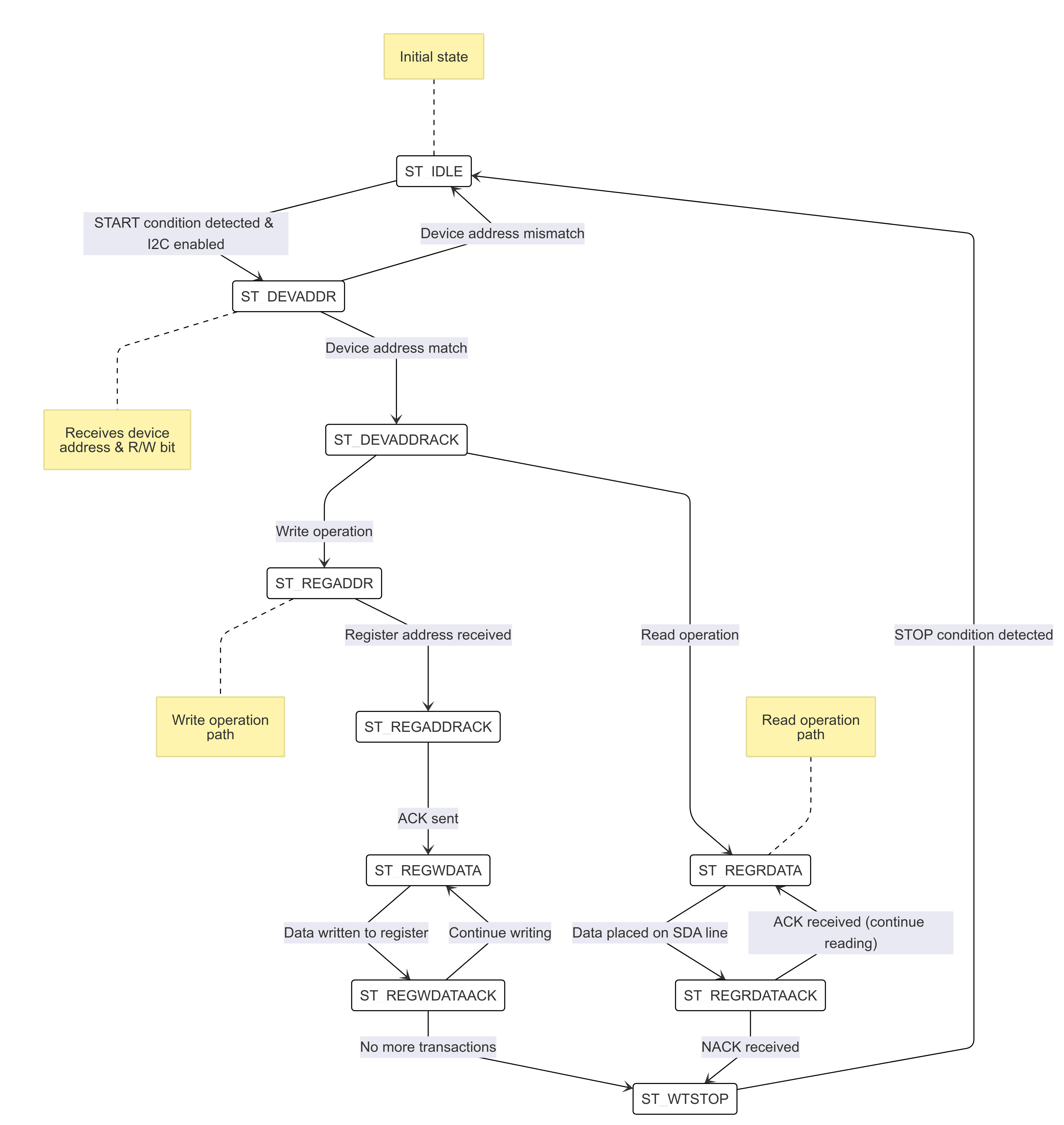
I2C Slave FSM Diagram
I2C slave has 10 states, :
- ST_IDLE:
Initially, the slave is in this state.
The slave may also return to this state if a STOP condition is detected.
- ST_DEVADDR:
The slave enters this state after detecting the START sequence and when I2C is enabled through the I2C enable CSR.
The slave receives the device address and transfer type (read/write).
8 bits are sent by the master over the SDA line(
i2c_sda_i), in which the first 7 represents the I2C slave device address and the 8th bit represents transfer type(1: Read, 0: Write).If the received device address does not match the configured address in the I2C device address CSR, the transaction is ignored.
- ST_DEVADDRACK:
After successfully validating the device address, the slave enters this state and sends an acknowledgment.
i2c_sda_o is driven low to indicate a successful acknowledgement.
The acknowledgment is released by driving i2c_sda_o high before a new transfer.
A read operation sets the I2C state to ST_REGRDATA.
A write operation sets the I2C state to ST_REGADDR.
- ST_REGADDR:
The slave comes to this state when the master writes the CSR address.
The I2C master sends the address of the target CSR located inside the I2C slave device over the SDA line(
i2c_sda_i).The slave receives this address to determine which CSR the master intends to write to.
- ST_REGADDRACK:
After successfully receiving the CSR address, the slave enters this state and sends an acknowledgment bit(ACK).
i2c_sda_o is driven low to indicate a successful acknowledgement.
The acknowledgment is released by driving i2c_sda_o high before a new transfer.
- ST_REGWDATA:
The slave enters this state if the master wants to write data to CSR.
Master sends the data to be written to the CSR over the SDA line(
i2c_sda_i).The slaves receives the data and then writes it to the intended CSR.
- ST_REGWDATAACK:
After successfully writing the data, an acknowledgment bit(ACK) is sent.
i2c_sda_o is driven low to indicate a successful acknowledgment.
The acknowledgment is released by driving i2c_sda_o high before a new transfer.
- ST_REGRDATA:
The slave enters this state if the master wants to read data from CSR.
The slave device places the data from the CSR, whose addressed was received in the previous ST_REGADDR phase, onto the i2c_sda_o line.
- ST_REGRDATAACK:
After a successful read, an acknowledgment is received.
If a negative acknowledgment(NACK) is received, the transfer stops.
If a successful acknowledgement(ACK) is received, then I2C state is set to ST_REGRDATA, and more data is read.
- ST_WTSTOP:
The slave enters this state if there are no more transactions or if the transfer is to be stopped.
Note: The master can stop the communication at any point during any of the above states by sending a stop condition. Whenever a stop condition is received the I2C slave goes into IDLE state.
System Architecture
The figure below depicts the connections between the I2C Slave and rest of the modules in CORE-V-MCU:-
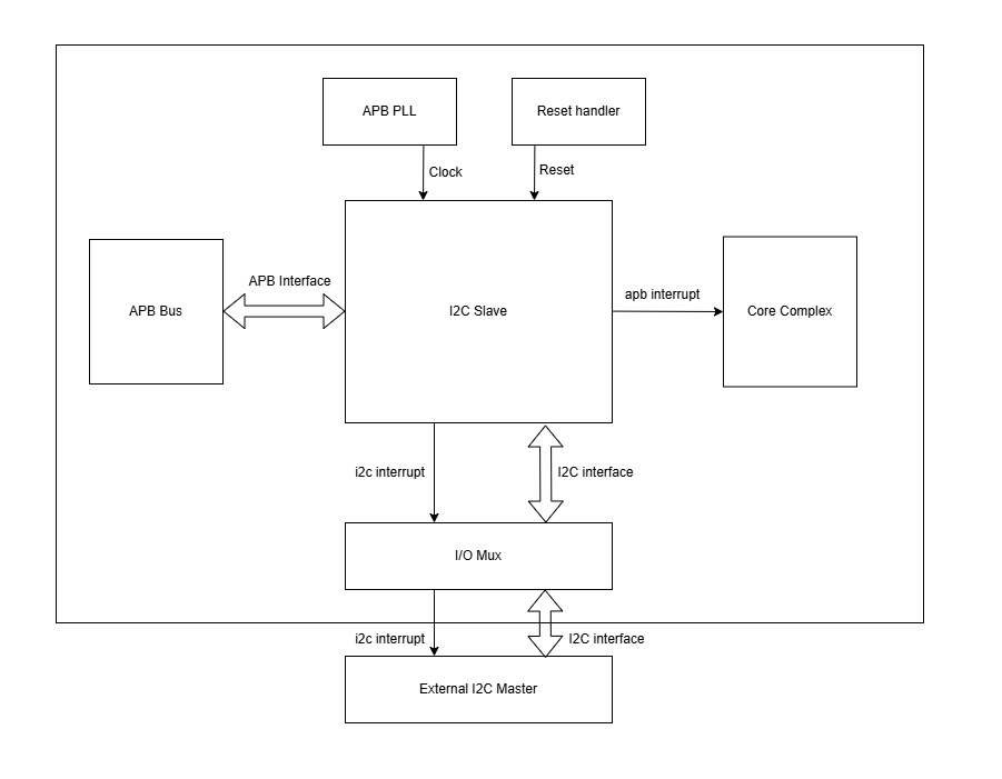
I2C Slave CORE-V-MCU connections diagram
Programming View Model
CSR Interaction
The CSRs are categorized based on their functionality:
Configuration CSRs:
Used to set up the I2C Slave module, including device address, debounce length, and delay parameters.
Example:
I2CS_DEV_ADDRESS,I2CS_ENABLE,I2CS_DEBOUNCE_LENGTH.
FIFO Management CSRs:
Facilitate data transfer between I2C and APB interfaces using FIFOs.
Example:
FIFO_I2C_TO_APB_WRITE_DATA_PORT,FIFO_APB_TO_I2C_READ_DATA_PORT.
Interrupt Control CSRs:
Enable and configure interrupts for efficient communication.
Example:
I2C_INTERRUPT_ENABLE,APB_INTERRUPT_ENABLE.
Status CSRs:
Provide real-time information about the module’s state, including FIFO flags and interrupt status.
Example:
FIFO_I2C_TO_APB_READ_FLAGS,I2C_INTERRUPT_STATUS.
Programming Guidelines
Initialization:
Configure the device address, debounce length, and delay parameters.
Enable the I2C Slave module and flush FIFOs.
Data Transfer:
Use single-byte or multi-byte communication modes based on application requirements.
Monitor FIFO flags to ensure proper data handling.
Interrupt Handling:
Enable interrupts for specific conditions.
Service interrupts by reading/writing appropriate CSRs.
FIFO Management:
Flush FIFOs when necessary to reset their state.
Monitor FIFO flags to prevent overflow or underflow.
RX and TX Operations
- RX Operation:
For single-byte RX, monitor the
MSG_I2C_TO_APB_STATUSCSR for new message availability and read the data fromMSG_I2C_TO_APB.For multi-byte RX, monitor the
FIFO_I2C_TO_APB_READ_FLAGSCSR for available data and read fromFIFO_I2C_TO_APB_READ_DATA_PORT.
- TX Operation:
For single-byte TX, write the data to
MSG_APB_TO_I2C.For multi-byte TX, monitor the
FIFO_APB_TO_I2C_WRITE_FLAGSCSR for available space and write data toFIFO_APB_TO_I2C_WRITE_DATA_PORT.
APB I2C Slave CSRs
The CSRs of the I2C slave are 8 bit CSRs mapped to a 32 bit APB data bus, the same CSRs can be accessed by the I2C interface as well. Since the APB bus is of 32 bit, the APB addresses are 4x the I2C addresses. For example, the I2CS_ENABLE CSR is at APB address 0x4, but at I2C address 0x1. Similarly, the I2CS_SCL_DELAY_LENGTH CSR is at APB address 0xC, but at I2C address 0x3.
Refer to Memory Map for the peripheral domain address of the I2C Slave which is used for APB bus addressing. NOTE: Several of the I2C Slave CSR are volatile, meaning that their read value may be changed by the hardware. For example, writing the FIFO_I2C_TO_APB_FLUSH CSR the value will be ignored and the FIFO will be flushed, but reading the CSR will return 0x0. As the name suggests, the value of non-volatile CSRs is not changed by the hardware. These CSRs retain the last value written by the software. A CSR’s volatility is indicated by its “type”. In I2C Slave the volatility of a CSR will also depend on the mode of access, i.e., whether it is accessed through the APB interface or the I2C interface.
I2CS_DEV_ADDRESS
APB Offset: 0x0
APB type: non-volatile
I2C Offset: 0x0
I2C type: volatile
Field |
Bits |
APB access type |
I2C access type |
Default |
Description |
|---|---|---|---|---|---|
RESERVED |
7:7 |
– |
– |
0x0 |
Reserved |
SLAVE_ADDR |
6:0 |
RW |
RO |
0X6F |
I2C device address |
I2CS_ENABLE
APB Offset: 0X4
APB type: non-volatile
I2C Offset: 0x1
I2C Type: volatile
Field |
Bits |
APB access type |
I2C access type |
Default |
Description |
|---|---|---|---|---|---|
RESERVED |
7:1 |
– |
– |
0x0 |
Reserved |
IP_ENABLE |
0:0 |
RW |
RO |
0X00 |
IP enabling bit 1: I2C slave is enabled 0: I2C slave is disabled I2C Slave operations(I2C FSM) can only work if this bit is set |
I2CS_DEBOUNCE_LENGTH
APB Offset: 0x8
APB type: non-volatile
I2C Offset: 0x2
I2C type: volatile
Field |
Bits |
APB access type |
I2C access type |
Default |
Description |
|---|---|---|---|---|---|
DEB_LEN |
7:0 |
RW |
RO |
0X14 |
Represents the number of system clocks over which each I2C line (SL and SDA) should be debounced. |
I2CS_SCL_DELAY_LENGTH
APB Offset: 0xC
APB type: non-volatile
I2C Offset: 0x3
I2C type: volatile
Field |
Bits |
APB access type |
I2C access type |
Default |
Description |
|---|---|---|---|---|---|
SCL_DLY_LEN |
7:0 |
RW |
RO |
0X14 |
Represents the number of system clocks over which the SCL line will be delayed relative to SDA line |
I2CS_SDA_DELAY_LENGTH
APB Offset: 0x10
APB type: non-volatile
I2C Offset: 0x4
I2C type: volatile
Field |
Bits |
APB access type |
I2C access type |
Default |
Description |
|---|---|---|---|---|---|
SDA_DLY_LEN |
7:0 |
RW |
RO |
0X08 |
Represents the number of system clocks over which the SDA line will be delayed relative to the SCL line. |
MSG_I2C_TO_APB
APB Offset: 0x40
APB type: volatile
I2C Offset: 0x10
I2C type: volatile
Field |
Bits |
APB access type |
I2C access type |
Default |
Description |
|---|---|---|---|---|---|
I2C_TO_APB |
7:0 |
RO |
RW |
0X0 |
This CSR provide a method for passing a single byte message from the I2C interface to the APB interface. |
MSG_I2C_TO_APB_STATUS
APB Offset: 0x44
APB type: volatile
I2C Offset: 0x11
I2C type: volatile
Field |
Bits |
APB access type |
I2C access type |
Default |
Description |
|---|---|---|---|---|---|
RESERVED |
7:1 |
– |
– |
0x0 |
|
I2C_TO_APB_STATUS |
0:0 |
RO |
RO |
0X0 |
This CSR indicates if a single byte message is available from I2C to APB. |
MSG_APB_TO_I2C
APB Offset: 0x48
APB type: non-volatile
I2C Offset: 0x12
I2C type: volatile
Field |
Bits |
APB access type |
I2C access type |
Default |
Description |
|---|---|---|---|---|---|
APB_TO_I2C |
7:0 |
RW |
RO |
0X0 |
This CSR provides a method for passing a single byte message from the APB interface to the I2C interface. |
MSG_APB_I2C_STATUS
APB Offset: 0x4C
APB type: volatile
I2C Offset: 0x13
I2C type: volatile
Field |
Bits |
APB access type |
I2C access type |
Default |
Description |
|---|---|---|---|---|---|
RESERVED |
7:1 |
– |
– |
0x0 |
|
APB_TO_I2C_STATUS |
0:0 |
RO |
RO |
0X0 |
This CSR indicates if a single byte message is available from APB to I2C. |
FIFO_I2C_TO_APB_WRITE_DATA_PORT
APB Offset: 0x80
APB type: NA
I2C Offset: 0x20
I2C type: non-volatile
Field |
Bits |
APB access type |
I2C access type |
Default |
Description |
|---|---|---|---|---|---|
I2C_APB_WRITE_DA TA_PORT |
7:0 |
– |
WO |
0x0 |
Not accessible by APB interface The I2C slave writes to this CSR when it wants to send multi-byte message. The data written to this CSR is pushed onto the I2C to APB FIFO. |
FIFO_I2C_TO_APB_READ_DATA_PORT
APB Offset: 0x084
APB type: volatile
I2C Offset: 0x21
I2C type: NA
Field |
Bits |
APB access type |
I2C access type |
Default |
Description |
|---|---|---|---|---|---|
I2C_APB_READ_DA TA_PORT |
7:0 |
RO |
– |
0x0 |
Not accessible by I2C interface The APB master reads from this CSR when it wants to retrieve multi-byte message from I2C to APB FIFO. Once the APB master reads this CSR, the data is popped from the I2C to APB FIFO. |
FIFO_I2C_TO_APB_FLUSH
APB Offset: 0x088
APB type: volatile
I2C Offset: 0x22
I2C type: volatile
Field |
Bits |
APB access type |
I2C access type |
Default |
Description |
|---|---|---|---|---|---|
RESERVED |
7:1 |
– |
– |
0x0 |
RESERVED |
ENABLE |
0:0 |
RW |
RW |
0x0 |
Writing a 1 to this CSR bit will flush the I2C to APB FIFO clearing all the contents and rendering the FIFO to be empty. |
FIFO_I2C_TO_APB_WRITE_FLAGS
APB Offset: 0x08C
APB type: volatile
I2C Offset: 0x23
I2C type: volatile
Field |
Bits |
APB access type |
I2C access type |
Default |
Description |
|---|---|---|---|---|---|
RESERVED |
7:3 |
– |
– |
0x0 |
RESERVED |
FLAGS |
2:0 |
RO |
RO |
0x0 |
Represent the number of spaces left in I2C TO APB FIFO in flags format. The flags range from 0 to 7 indicating different levels of available space in FIFO. Flag Value descriptions:
|
FIFO_I2C_TO_APB_READ_FLAGS
APB Offset: 0x90
APB type: volatile
I2C Offset: 0x24
I2C type: volatile
Field |
Bits |
APB access type |
I2C access type |
Default |
Description |
|---|---|---|---|---|---|
RESERVED |
7:3 |
– |
– |
0x0 |
RESERVED |
FLAGS |
2:0 |
RO |
RO |
0x0 |
Represent the items present in FIFO to read in I2C TO APB FIFO in flags The flags range from 0 to 7 indicating different levels of items present in FIFO. Flag Value descriptions:
|
FIFO_APB_TO_I2C_WRITE_DATA_PORT
APB Offset: 0XC0
APB type: non-volatile
I2C Offset: 0x30
I2C type: NA
Field |
Bits |
APB access type |
I2C access type |
Default |
Description |
|---|---|---|---|---|---|
I2C_APB_WRITE_DA TA_PORT |
7:0 |
WO |
– |
0x0 |
Not accessible by I2C interface The APB master writes to this CSR when it wants to send multi-byte message. The data written to this CSR is pushed onto the APB to I2C FIFO. |
FIFO_APB_TO_I2C_READ_DATA_PORT
APB Offset: 0XC4
APB type: NA
I2C Offset: 0x31
I2C type: volatile
Field |
Bits |
APB access type |
I2C access type |
Default |
Description |
|---|---|---|---|---|---|
I2C_APB_READ_DA TA_PORT |
7:0 |
– |
RO |
0x0 |
Not accessible by APB interface The I2C master reads from this CSR when it wants to retrieve multi-byte message from APB to I2C FIFO. Once the I2C master reads this CSR, the data is popped from the APB to I2C FIFO. |
FIFO_APB_TO_I2C_FLUSH
APB Offset: 0XC8
APB type: volatile
I2C Offset: 0x32
I2C type: volatile
Field |
Bits |
APB access type |
I2C access type |
Default |
Description |
|---|---|---|---|---|---|
RESERVED |
7:1 |
– |
– |
0x0 |
RESERVED |
ENABLE |
0:0 |
RW |
RW |
0x0 |
Writing a 1 to this CSR bit will flush the APB to I2C FIFO, clearing all contents and rendering the FIFO to be empty. |
FIFO_APB_TO_I2C_WRITE_FLAGS
APB Offset: 0XCC
APB type: volatile
I2C Offset: 0x33
I2C type: volatile
Field |
Bits |
APB access type |
I2C access type |
Default |
Description |
|---|---|---|---|---|---|
RESERVED |
7:3 |
– |
– |
0x0 |
|
FLAGS |
2:0 |
RO |
RO |
0x0 |
Represent number of spaces left in APB TO I2C FIFO in flags format. The flags range from 0 to 7 indicating different levels of available space in FIFO. NOTE: For flag value description please refer to FIFO_I2C_TO_APB_WRITE_FLAGS CSR |
FIFO_APB_TO_I2C_READ_FLAGS
APB Offset: 0XD0
APB type: volatile
I2C Offset: 0x34
I2C type: volatile
Field |
Bits |
APB access type |
I2C access type |
Default |
Description |
|---|---|---|---|---|---|
RESERVED |
7:3 |
– |
– |
0x0 |
|
FLAGS |
2:0 |
RO |
RO |
0x0 |
Represent the items present in APB TO I2C FIFO to read. The flags range from 0 to 7 indicating different levels of items present in FIFO. NOTE: For flag value description please refer to FIFO_I2C_TO_APB_READ_FLAGS CSR |
I2C_INTERRUPT_STATUS
APB Offset: 0x100
APB type: volatile
I2C Offset: 0x40
I2C type: volatile
Field |
Bits |
APB access type |
I2C access type |
Default |
Description |
|---|---|---|---|---|---|
RESERVED |
7:3 |
– |
– |
0x0 |
Reserved |
I2C_APB_F IFO_WRITE_STATUS |
2:2 |
RO |
RO |
0x0 |
1: Interrupt is generated for this field 0: Not genertated Indicates if interrupt is generated for the I2C to APB FIFO write flags. |
APB_I2C_F IFO_READ_STATUS |
1:1 |
RO |
RO |
0x0 |
1: Interrupt is generated for this field 0: Not genertated Indicates if interrupt is generated for the APB to I2C FIFO read flags. |
APB_I2C_M ESSAGE_AVAILABLE |
0:0 |
RO |
RO |
0x0 |
1: Interrupt is generated for this field 0: Not genertated Indicates if interrupt is generated for the I2C to APB message available status. |
I2C_INTERRUPT_ENABLE
APB Offset: 0x104
APB type: volatile
I2C Offset: 0x41
I2C type: non-volatile
Field |
Bits |
APB access type |
I2C access type |
Default |
Description |
|---|---|---|---|---|---|
RESERVED |
7:3 |
– |
– |
0x0 |
Reserved |
I2C_A PB_FIFO_WRITE_S TATUS_INT_ENABLE |
2:2 |
RO |
RW |
0x0 |
1: enabled 0: disabled This field enables the interrupt for the I2C to APB FIFO write flags. |
APB_I2C_F IFO_READ_S TATUS_INT_ENABLE |
1:1 |
RO |
RW |
0x0 |
1: enabled 0: disabled This field enables the interrupt for the APB to I2C FIFO read flags. |
APB_I2C_M ESSAGE_AVAI LABLE_INT_ENABLE |
0:0 |
RO |
RW |
0x0 |
1: enabled 0: disabled This field enables the interrupt for the I2C to APB message available status. |
INTERRUPT_FIFO_I2C_TO_APB_WRITE_FLAGS_SELECT
APB Offset: 0x108
APB type: volatile
I2C Offset: 0x42
I2C type: non-volatile
Field |
Bits |
APB access type |
I2C access type |
Default |
Description |
|---|---|---|---|---|---|
WRITE_FLAG_FULL |
7:7 |
RO |
RW |
0x0 |
If this bit is set, then interrupt will be generated when the I2C to APB FIFO is full, given that the write flags interrupt is enabled. |
WRITE_FL AG_1_SPACE_AVAIL |
6:6 |
RO |
RW |
0x0 |
If this bit is set, then interrupt will be generated when there is 1 space available in the I2C to APB FIFO, given that the write flags interrupt is enabled. |
WRITE_FLAG _2_3_SPACE_AVAIL |
5:5 |
RO |
RW |
0x0 |
If this bit is set, then interrupt will be generated when there are 2-3 spaces available in the I2C to APB FIFO, given that the write flags interrupt is enabled. |
WRITE_FLAG _4_7_SPACE_AVAIL |
4:4 |
RO |
RW |
0x0 |
If this bit is set, then interrupt will be generated when there are 4-7 spaces available in the I2C to APB FIFO, given that the write flags interrupt is enabled. |
WRITE_FLAG _8_31_SPACE_AVAIL |
3:3 |
RO |
RW |
0x0 |
If this bit is set, then interrupt will be generated when there are 8-31 spaces available in the I2C to APB FIFO, given that the write flags interrupt is enabled. |
WRITE_FLAG_3 2_63_SPACE_AVAIL |
2:2 |
RO |
RW |
0x0 |
If this bit is set, then interrupt will be generated when there are 32-63 spaces available in the I2C to APB FIFO, given that the write flags interrupt is enabled. |
WRITE_FLAG_64 _127_SPACE_AVAIL |
1:1 |
RO |
RW |
0x0 |
If this bit is set, then interrupt will be generated when there are 64-127 spaces available in the I2C to APB FIFO, given that the write flags interrupt is enabled. |
WRITE_FLAG_1 28__SPACE_AVAIL |
0:0 |
RO |
RW |
0x0 |
If this bit is set, then interrupt will be generated when there are more than 127 spaces available in the I2C to APB FIFO, given that the write flags interrupt is enabled. |
INTERRUPT_FIFO_APB_TO_I2C_READ_FLAGS_SELECT
APB Offset: 0x10C
APB type: volatile
I2C Offset: 0x43
I2C type: non-volatile
Field |
Bits |
APB access type |
I2C access type |
Default |
Description |
|---|---|---|---|---|---|
READ_FLAG _128_SPACE_AVAIL |
7:7 |
RO |
RW |
0x0 |
If this bit is set, then interrupt will be generated when the APB To I2C FIFO has more than 127 items, given that the read flags interrupt is enabled. |
READ_FLAG_64 _127_SPACE_AVAIL |
6:6 |
RO |
RW |
0x0 |
If this bit is set, then interrupt will be generated when the APB To I2C FIFO has 64-127 items, given that the read flags interrupt is enabled. |
READ_FLAAG_3 2_63_SPACE_AVAIL |
5:5 |
RO |
RW |
0x0 |
If this bit is set, then interrupt will be generated when the APB To I2C FIFO has 32-63 items, given that the read flags interrupt is enabled. |
READ_FLAG_8 _31_SPACE_AVAIL |
4:4 |
RO |
RW |
0x0 |
If this bit is set, then interrupt will be generated when the APB To I2C FIFO has 8-31 items, given that the read flags interrupt is enabled. |
READ_FLAG _4_7_SPACE_AVAIL |
3:3 |
RO |
RW |
0x0 |
If this bit is set, then interrupt will be generated when the APB To I2C FIFO has 4-7 items, given that the read flags interrupt is enabled. |
READ_FLAG _2_3_SPACE_AVAIL |
2:2 |
RO |
RW |
0x0 |
If this bit is set, then interrupt will be generated when the APB To I2C FIFO has 2-3 items, given that the read flags interrupt is enabled. |
READ_FL AG_1_SPACE_AVAIL |
1:1 |
RO |
RW |
0x0 |
If this bit is set, then interrupt will be generated when there is 1 item available in the APB To I2C FIFO, given that the read flags interrupt is enabled. |
READ_FLAG_EMPTY |
0:0 |
RO |
RW |
0x0 |
If this bit is set, then interrupt will be generated when the APB To I2C FIFO is empty, given that the read flags interrupt is enabled. |
APB_INTERRUPT_STATUS
APB Offset: 0x140
APB type: volatile
I2C Offset: 0x50
I2C type: volatile
Field |
Bits |
APB access type |
I2C access type |
Default |
Description |
|---|---|---|---|---|---|
RESERVED |
7:3 |
– |
– |
0x0 |
Reserved |
APB_I2C_F IFO_WRITE_STATUS |
2:2 |
RO |
RO |
0x0 |
1: Interrupt is generated 0: Not genertated Indicates if interrupt is generated for APB to I2C FIFO write flags. |
I2C_APB_F IFO_READ_STATUS |
1:1 |
RO |
RO |
0x0 |
1: Interrupt is generated 0: Not genertated Indicates if interrupt is generated for APB to I2C FIFO read flags. |
NEW_I 2C_APB_MSG_AVAIL |
0:0 |
RO |
RO |
0x0 |
1: Interrupt is generated 0: Not genertated Indicates if interrupt is generated for I2C to APB message available status. |
APB_INTERRUPT_ENABLE
APB Offset: 0x144
APB type: non-volatile
I2C Offset: 0x51
I2C type: volatile
Field |
Bits |
APB access type |
I2C access type |
Default |
Description |
|---|---|---|---|---|---|
RESERVED |
7:3 |
– |
– |
0x0 |
Reserved |
APB_I2C_FIFO_WRI TE_STATUS_ENABLE |
2:2 |
RW |
RO |
0x0 |
1: enabled 0: disabled This field enables the interrupt for the APB to I2C FIFO write flags. |
I2C_APB_FIFO_RE AD_STATUS_ENABLE |
1:1 |
RW |
RO |
0x0 |
1: enabled 0: disabled This field enables the interrupt for the I2C to APB FIFO read flags. |
NEW_I2C_APB_M SG_AVAIL_ENABLE |
0:0 |
RW |
RO |
0x0 |
1: enabled 0: disabled This field enables the interrupt for the I2C to APB message available status. |
INTERRUPT_FIFO_APB_TO_I2C_WRITE_FLAGS_SELECT
APB Offset: 0x148
APB type: non-volatile
I2C Offset: 0x52
I2C type: volatile
Field |
Bits |
APB access type |
I2C access type |
Default |
Description |
|---|---|---|---|---|---|
WRITE_FLAG_FULL |
7:7 |
RO |
RW |
0x0 |
If this bit is set, then interrupt will be generated when the APB to I2C FIFO is full, given that the write flags interrupt is enabled. |
WRITE_FL AG_1_SPACE_AVAIL |
6:6 |
RO |
RW |
0x0 |
If this bit is set, then interrupt will be generated when there is 1 space available in the APB to I2C FIFO, given that the write flags interrupt is enabled. |
WRITE_FLAG _2_3_SPACE_AVAIL |
5:5 |
RO |
RW |
0x0 |
If this bit is set, then interrupt will be generated when there are 2-3 spaces available in the APB to I2C FIFO, given that the write flags interrupt is enabled. |
WRITE_FLAG _4_7_SPACE_AVAIL |
4:4 |
RO |
RW |
0x0 |
If this bit is set, then interrupt will be generated when there are 4-7 spaces available in the APB to I2C FIFO, given that the write flags interrupt is enabled. |
WRITE_FLAG _8_31_SPACE_AVAIL |
3:3 |
RO |
RW |
0x0 |
If this bit is set, then interrupt will be generated when there are 8-31 spaces available in the APB to I2C FIFO, given that the write flags interrupt is enabled. |
WRITE_FLAG_3 2_63_SPACE_AVAIL |
2:2 |
RO |
RW |
0x0 |
If this bit is set, then interrupt will be generated when there are 32-63 spaces available in the APB to I2C FIFO, given that the write flags interrupt is enabled. |
WRITE_FLAG_64 _127_SPACE_AVAIL |
1:1 |
RO |
RW |
0x0 |
If this bit is set, then interrupt will be generated when there are 64-127 spaces available in the APB to I2C FIFO, given that the write flags interrupt is enabled. |
WRITE_FLAG_1 28__SPACE_AVAIL |
0:0 |
RO |
RW |
0x0 |
If this bit is set, then interrupt will be generated when there are more than 127 spaces available in the APB to I2C FIFO, given that the write flags interrupt is enabled. |
INTERRUPT_FIFO_I2C_TO_APB_READ_FLAGS_SELECT
APB Offset: 0x14C
APB type: non-volatile
I2C Offset: 0x53
I2C type: volatile
Field |
Bits |
APB access type |
I2C access type |
Default |
Description |
|---|---|---|---|---|---|
READ_FLAG _128_SPACE_AVAIL |
7:7 |
RO |
RW |
0x0 |
If this bit is set, then interrupt will be generated when the I2C to APB FIFO has more than 127 items, given that the read flags interrupt is enabled. |
READ_FLAG_64 _127_SPACE_AVAIL |
6:6 |
RO |
RW |
0x0 |
If this bit is set, then interrupt will be generated when the I2C to APB FIFO has 64-127 items, given that the read flags interrupt is enabled. |
READ_FLAAG_3 2_63_SPACE_AVAIL |
5:5 |
RO |
RW |
0x0 |
If this bit is set, then interrupt will be generated when the I2C to APB FIFO has 32-63 items, given that the read flags interrupt is enabled. |
READ_FLAG_8 _31_SPACE_AVAIL |
4:4 |
RO |
RW |
0x0 |
If this bit is set, then interrupt will be generated when the I2C to APB FIFO has 8-31 items, given that the read flags interrupt is enabled. |
READ_FLAG _4_7_SPACE_AVAIL |
3:3 |
RO |
RW |
0x0 |
If this bit is set, then interrupt will be generated when the I2C to APB FIFO has 4-7 items, given that the read flags interrupt is enabled. |
READ_FLAG _2_3_SPACE_AVAIL |
2:2 |
RO |
RW |
0x0 |
If this bit is set, then interrupt will be generated when the I2C to APB FIFO has 2-3 items, given that the read flags interrupt is enabled. |
READ_FL AG_1_SPACE_AVAIL |
1:1 |
RO |
RW |
0x0 |
If this bit is set, then interrupt will be generated when there is 1 item available in the I2C to APB FIFO, given that the read flags interrupt is enabled. |
READ_FLAG_EMPTY |
0:0 |
RO |
RW |
0x0 |
If this bit is set, then interrupt will be generated when the I2C to APB FIFO is empty, given that the read flags interrupt is enabled. |
Firmware Guidelines
Initialization
Set the I2C device address in the I2C device address CSR.
Configure appropriate debounce and delay values for SCL and SDA lines through
I2CS_DEBOUNCE_LENGTH,I2CS_SCL_DELAY_LENGTHandI2CS_SDA_DELAY_LENGTHCSRs.Set the appropriate interrupt enable bits in the
APB_INTERRUPT_ENABLECSR for APB to I2C communication andI2C_INTERRUPT_ENABLECSR for I2C to APB communication.Configure the FIFO read flags and write flags in
INTERRUPT_FIFO_I2C_TO_APB_READ_FLAGS_SELECTandINTERRUPT_FIFO_APB_TO_I2C_WRITE_FLAGS_SELECTCSRs respectively, to set the desired interrupt levels.Flush the FIFOs by writing 1 to
FIFO_I2C_TO_APB_FLUSHandFIFO_APB_TO_I2C_FLUSHCSRs to ensure they are empty before starting communication.Enable the I2C interface by writing 1 to the
I2CS_ENABLECSR.
I2C Slave Single-Byte Communication
- TX Operation:
Write the data byte to the
MSG_APB_TO_I2CCSR.The
i2c_interrupt_osignal will be asserted (depending upon the interrupt configurtion by the external I2C master) and the external I2C master can then take the appropriate actions.
- RX Operation:
Configure the
APB_INTERRUPT_ENABLECSR to enable the interrupt for new message availability (Bit 0).Monitor the
apb_interrupt_osignal, the signal will be asserted when a new message is available or when the FIFO read flags match the specified pattern.When the signal is asserted check the
MSG_I2C_TO_APB_STATUSCSR’sNEW_I2C_APB_MSG_AVAILbit(Bit 0) to check if the interrupt was generated due to a new message.If it was generated due to new message, read the data byte from the
MSG_I2C_TO_APBCSR.The status bit in
MSG_I2C_TO_APB_STATUSis cleared automatically after the data is read.
I2C Slave Multi-Byte Communication
- TX Operation:
Monitor the
FIFO_APB_TO_I2C_WRITE_FLAGSCSR to ensure there is space available in the FIFO.If space is available, write the data to the
FIFO_APB_TO_I2C_WRITE_DATA_PORTCSR.The
i2c_interrupt_osignal will be asserted (depending upon the interrupt configurtion by the external I2C master) and the external I2C master can then take the appropriate actions.
- RX Operation:
Configure the
APB_INTERRUPT_ENABLECSR to enable the interrupt for FIFO read flags (Bit 1).- Configure the
INTERRUPT_FIFO_I2C_TO_APB_READ_FLAGS_SELECTCSR to set the read flags for FIFO read interrupts, to the desired values. For example, to generate an interrupt when there are 64-127 items available in the FIFO, set Bit 6 in
INTERRUPT_FIFO_I2C_TO_APB_READ_FLAGS_SELECT.Multiple bits can be set to generate interrupts for multiple levels of data availability.
- Configure the
Monitor the
apb_interrupt_osignal, the signal will be asserted when the FIFO read flags match the specified pattern.When the signal is asserted, check the
FIFO_I2C_TO_APB_READ_FLAGSCSR to determine the number of items available in the FIFO.- Read the data from the
FIFO_I2C_TO_APB_READ_DATA_PORTCSR. 8 Bits of data can be read at a time.
Each read will pop the data from the FIFO and the next data will be available for reading on the CSR port.
- Read the data from the
The FIFO status(flags) is updated automatically after the data is read.
FIFO Management
FIFO Operations
- FIFOs can be flushed by writing 1 to
FIFO_I2C_TO_APB_FLUSHCSR (I2C to APB FIFO) orFIFO_APB_TO_I2C_FLUSHCSR (APB to I2C FIFO).
Flushing clears all contents of the FIFO and resets its status flags.
Ensure that the FIFO is not actively being read or written during the flush operation to avoid data corruption.
- Monitor FIFO read and write status flags to prevent overflow/underflow conditions.
Use
FIFO_I2C_TO_APB_READ_FLAGSCSR to check the current read flags for the I2C to APB FIFO.Use
FIFO_APB_TO_I2C_READ_FLAGSCSR to check the current read flags for the APB to I2C FIFO.Use
FIFO_I2C_TO_APB_WRITE_FLAGSCSR to check the current write flags for the I2C to APB FIFO.Use
FIFO_APB_TO_I2C_WRITE_FLAGSCSR to check the current write flags for the APB to I2C FIFO.
Interrupt Management
Interrupt Configuration for single-byte communication
- Configure interrupts to trigger when a new single byte message is available by setting the appropriate bit in the:
APB_INTERRUPT_ENABLECSR for APB to I2C communication.
I2C_INTERRUPT_ENABLECSR for I2C to APB communication.Refer to the respective CSR descriptions for further details on configuration.
Interrupt Configuration for multi-byte communication
Configure interrupts to trigger based on FIFO read and write flags or new message availability.
- Use the following CSRs for configuration:
INTERRUPT_FIFO_I2C_TO_APB_READ_FLAGS_SELECTfor I2C to APB FIFO read flags.
INTERRUPT_FIFO_APB_TO_I2C_READ_FLAGS_SELECTfor APB to I2C FIFO read flags.
INTERRUPT_FIFO_I2C_TO_APB_WRITE_FLAGS_SELECTfor I2C to APB FIFO write flags.
INTERRUPT_FIFO_APB_TO_I2C_WRITE_FLAGS_SELECTfor APB to I2C FIFO write flags.Refer to the respective CSR descriptions for further details on configuration.
Interrupt Handling
The external I2C device should monitor the interrupt i2c_interrupt_o for I2C interrupts. Whereas the firmware should monitor the interrupt apb_interrupt_o for APB interrupts.
- When an interrupt is triggered, the following steps should be taken either by the external I2C device or the firmware depending on the interrupt:
- Read the interrupt status CSR:
Determine the interrupt source using bitfields of
I2C_INTERRUPT_STATUSCSR for I2C interrupts.Determine the interrupt source using bitfields of
APB_INTERRUPT_STATUSCSR for APB interrupts.
- Service the interrupt by reading/writing appropriate data:
For new message availability, read the corresponding CSR (
MSG_I2C_TO_APBorMSG_APB_TO_I2C) to deassert the interrupt and clear the respective status CSRs.For FIFO read flags, read data from the FIFO read data port CSR (
FIFO_I2C_TO_APB_READ_DATA_PORTorFIFO_APB_TO_I2C_READ_DATA_PORT) to deassert the interrupt and clear the respective status CSRs.For FIFO write flags, write data to the FIFO write data port CSR (
FIFO_I2C_TO_APB_WRITE_DATA_PORTorFIFO_APB_TO_I2C_WRITE_DATA_PORT) to deassert the interrupt and clear the respective status CSRs.
Pin Diagram
The figure below represents the input and output pins for the I2C Slave:-
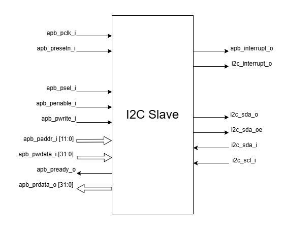
I2C Slave Pin Diagram
Clock and Reset Signals
apb_pclk_i: System clock input
apb_presetn_i: Active-low reset input
APB Interface Signals
apb_paddr_i[11:0]: APB address bus input
apb_psel_i: APB peripheral select input
apb_penable_i: APB enable input
apb_pwrite_i: APB write control input (high for write, low for read)
apb_pwdata_i[31:0]: APB write data bus input
apb_pready_o: APB ready output to indicate transfer completion
apb_prdata_o[31:0]: APB read data bus output
I2C Interface Signals
i2c_scl_i: I2C clock input
i2c_sda_i: I2C data input
i2c_sda_o: I2C data output
i2c_sda_oe: I2C data output enable (active high)
Note: At the top level of the CORE-V-MCU, these internal I2C signals map to two external I2C signals provided through IO pads:
i2c_scl_iconnects directly toi2cs_scl(clock line)i2cs_sda(data line) is formed by combiningi2c_sda_iandi2c_sda_o, wherei2c_sda_oecontrols the direction: - Wheni2c_sda_oeis high:i2cs_sdaoutputsi2c_sda_o- Wheni2c_sda_oeis low:i2cs_sdafeeds intoi2c_sda_i
Interrupt Signals
i2c_interrupt_o: I2C interrupt request output, connects to external I2C master
apb_interrupt_o: APB interrupt request output, connects to Core-Complex